
Adhesion promotion for etch by-products

a technology of adhesion promotion and by-products, which is applied in the direction of cleaning process and apparatus, cleaning liquids, chemical instruments and processes, etc., can solve the problems of component failure, high cost, and high cost of components, and achieves the effects of low cost, simple process, and high efficiency

Inactive Publication Date: 2007-02-13
NOVELLUS SYSTEMS
View PDF4 Cites 13 Cited by
  • Summary
  • Abstract
  • Description
  • Claims
  • Application Information

AI Technical Summary

Benefits of technology

[0012]It is another object of the present invention to provide a method and assembly for preventing residues, by-products, contaminants and / or molecular fragments from damaging any semiconductor substrates being processed within a process chamber.
[0013]A further object of the invention is to provide a method and assembly for cleaning semiconductor substrate surfaces that is easy, efficient, effective, inexpensive and reliable.
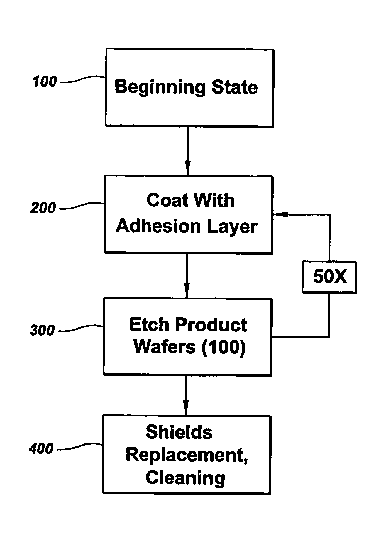
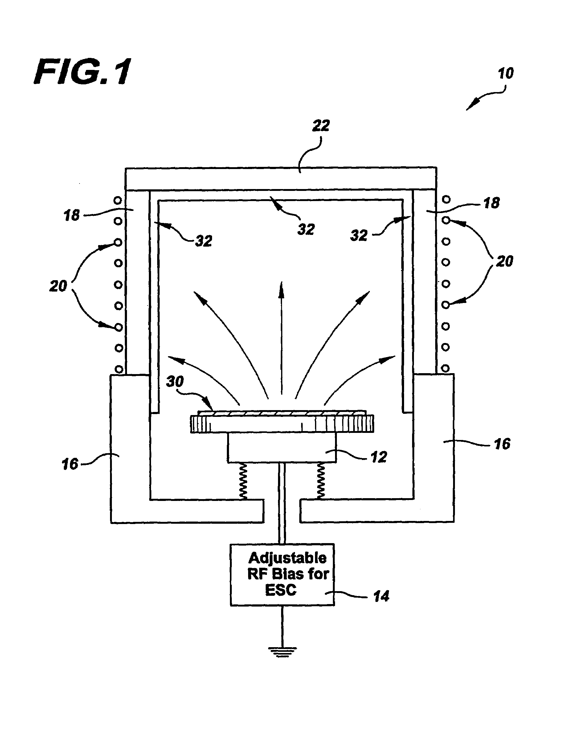
[0022]In still another aspect, the invention is directed to an apparatus for cleaning a semiconductor substrate. The apparatus includes a processing chamber having a plurality of interior components, and an adhesion film coating all interior surfaces within the processing chamber including surfaces of the interior components. A critical feature of this adhesion film is that it has a sufficient sticking coefficient for adherence of materials removed from at least one semiconductor substrate for cleaning the semiconductor substrate in order to promote a continuous film growth of the removed materials and improve adhesion of the film on the adhesion film. Optionally, the apparatus may include a plurality of adhesion films sequentially deposited over a plurality of continuous film growths of the removed materials for cleaning a plurality semiconductor substrates.

Problems solved by technology

The fabrication of electronic components such as integrated circuit semiconductors is very exacting and complex and requires a number of processing steps requiring extreme precision to form the desired circuit pattern on the component substrate.
Contamination of the semiconductor substrate in the form of particles on the substrate surface may cause short circuits, open circuits and other defects, which can cause the component to fail and / or adversely affect the performance of the component.
For example, an individual particle as small as 100 angstroms in diameter can result in a defect in a modern microcircuit electronic component.
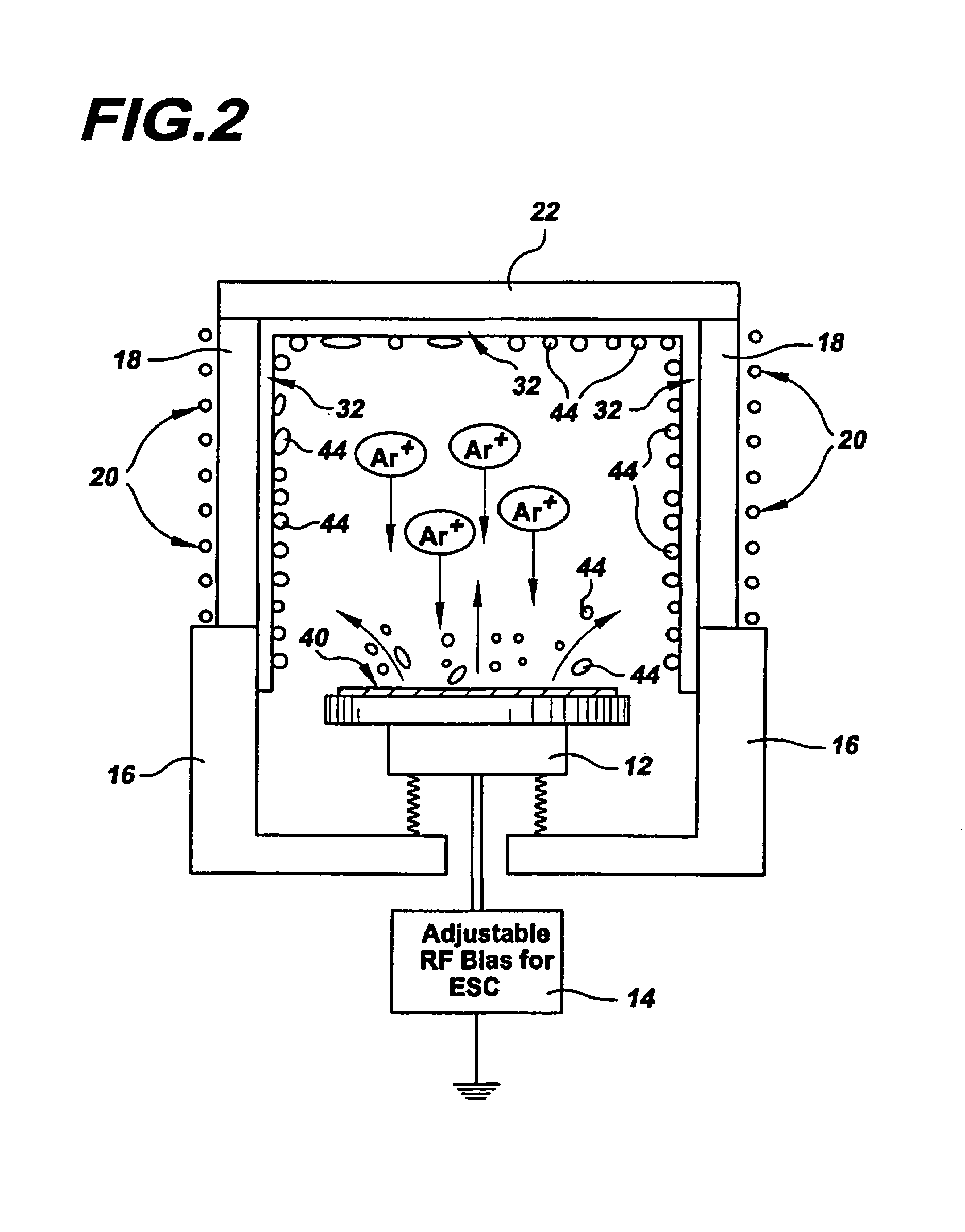
As these by-products, residues and particles are sputtered, they adhere to the chamber components and interior chamber surfaces in a non-uniform manner.
Due to this non-uniform nature of adherence, the deposited by-products, residues and particles have relatively poor adhesion to the chamber walls and components since the areas of contact and bonding between deposition and the chamber walls and components are small.
However, rather than forming a continuous coating or film, upon contact of these by-products, residues and / or particle nodules with each other, the nodules crack and break-off due to the low ductility, falling onto the semiconductor wafer being processed.
It is these particles falling onto the semiconductor surfaces that damage the semiconductor and ultimately lead to device failure.
One root cause of particle failure is believed to be due to poor adhesion of by-products to the chamber components and interior surfaces due to small areas of contact and bonding.
However, such practices do not significantly improve material delamination, such that these procedures are not sufficient for practical production and manufacturing purposes.
Wafer contamination continues to be a problem in the electronics and semiconductor fabrication industry.

Method used


Image

  • Adhesion promotion for etch by-products
  • Adhesion promotion for etch by-products
  • Adhesion promotion for etch by-products

Examples


Embodiment Construction

)

[0030]In describing the preferred embodiment of the present invention, reference will be made herein to FIGS. 1–6 of the drawings in which like numerals refer to like features of the invention.

[0031]The present invention significantly reduces the number of particles that deposit on a wafer or semiconductor substrate during the cleaning or precleaning stage by coating all interior surfaces within the processing chamber with a continuous material that increases the sticking coefficient of any arriving etched species to promote a continuous film growth and improve the adhesion of such etched species. The invention enables accumulation of significantly thicker etched species depositions without an on-wafer particle failure. An advantage of the present invention is that the increased sticking characteristics of the continuous pre-coating and post-coating films of the invention reduce surface mobility of any arriving by-products such that a continuous film growth is promoted. An advantag...


PUM

PropertyMeasurementUnit
thicknessaaaaaaaaaa
widthsaaaaaaaaaa
diameteraaaaaaaaaa

Abstract

Methods and apparatus for cleaning a semiconductor substrate that significantly reduce the number of particles falling onto the substrate during cleaning by coating all interior surfaces within a processing chamber with an adhesion film that has an increased sticking coefficient for any subsequently arriving etched species to promote a continuous film growth and improve adhesion of such etched species. Due to its increased sticking coefficient, this adhesion film reduces surface mobility of any arriving by-products to enable the growth of the continuous film of etched species. The continuous film of etched species adheres firmly to the adhesion film such that the etched species are prevented from flaking off and falling onto the substrate being cleaned. The methods and apparatus may clean a plurality of semiconductor substrates, whereby a plurality of adhesion films are sequentially deposited over a plurality of continuous film growths of removed materials for cleaning the substrates.

Description

BACKGROUND OF THE INVENTION[0001]1. Field of the Invention[0002]The present invention relates generally to the cleaning of residues and by-products from substrate surfaces and, in particular, to removing residues and by-products from electronic component substrates, such as integrated circuits and semiconductor wafers, and adhering such removed residues and by-products to interior surfaces within a processing chamber.[0003]2. Description of Related Art[0004]The fabrication of electronic components such as integrated circuit semiconductors is very exacting and complex and requires a number of processing steps requiring extreme precision to form the desired circuit pattern on the component substrate. Typical semiconductor devices now have circuit line widths typically less than 0.5 micron with close spacing of the lines and via interconnections. Contamination of the semiconductor substrate in the form of particles on the substrate surface may cause short circuits, open circuits and ot...

Claims


Application Information

Patent Timeline
Patent Type & Authority Patents(United States)
IPC IPC(8): H01L21/302H01L21/3065
CPCH01L21/02057
Inventor RIVKIN, MICHAELFAIR, JAMES A
Owner NOVELLUS SYSTEMS
Learn More