Push-pull inverter with snubber energy recovery

a technology of push-pull inverter and energy recovery, which is applied in the direction of power conversion systems, dc-dc conversion, electrical equipment, etc., can solve the problems of snubbing circuit, increasing the cost and size of inverter circuit, and reducing the efficiency of inverter circuits

Active Publication Date: 2007-02-20
SQUARE D CO
View PDF6 Cites 16 Cited by
  • Summary
  • Abstract
  • Description
  • Claims
  • Application Information

AI Technical Summary

Benefits of technology

[0006]The present invention provides an apparatus and method for improving, among other things, the design, construction, packaging, and operation of power inverters that make use of push-pull inverter circuits for DC-to-AC power conversion. According to one or more exemplary embodiments of the present invention, the same transformer used for DC-to-AC power conversion in the push-pull inverter circuit is also used for DC-to-DC power conversion operations associated with recovering energy from a snubber circuit of the power inverter. Using the DC-to-AC converter's transformer inductance for DC-to-DC power conversion between the snubber bus and the DC bus of the power inverter obviates the need for adding separate inductor elements to effect snubber energy recovery.
[0009]While implementing both the first and second DC-to-DC converters offers certain advantages, such as additional flexibility in controlling the snubber bus energy return process, those skilled in the art should note that the present invention contemplates embodiments having only one DC-to-DC converter. That is, snubber energy can be recovered by forming just one DC-to-DC converter circuit, i.e., by adding just one supplemental switch at a given end of the push-pull inverter circuit transformer's primary winding.
[0011]Further, the transistor switches can comprise one or more commercially packaged circuit devices, which often include reverse-parallel diodes in the same device package. In such cases, these included diodes can serve as the required free-wheeling and snubber diodes, thus eliminating the need to include separately packaged diodes. Of course, it should be understood that the transistor switches need not include integral diodes, and that separate transistor switches and diodes can be used according to design needs. Also, it should be noted that the main power switches and supplemental switches can be integrated together in a full-bridge transistor circuit for additional size, space, and packaging improvements.
[0012]Regardless, one or more embodiments of the present invention further comprise switching control logic, which can be implemented in a switching controller circuit that controls the conduction timing (on-timing) of the included switches in coordinated fashion to effect the desired power inverter operation. By controlling the on-times of the main power switches, i.e., the first and second switches at opposite ends of the inverter circuit transformer's primary winding, switching control can effect the desired DC-to-AC conversion, and by overlapping the turn-on times of the first and second switches by a controlled amount, additionally can provide boost-mode operation wherein power flows from the inverter circuit to the snubber circuit. Such operation is advantageous where the snubber circuit includes batteries or the like.
[0013]Further, of particular interest herein, by controlling the on-times of the supplemental switch, or switches, i.e., the added high-side switches coupling the primary winding to the snubber bus, switching control can operate the DC-to-DC converters formed by the addition of those supplemental switches as buck converters that recover energy from the snubber circuit. That is, the third and fourth switches described above can be operated by the switching control logic such that the intrinsically formed DC-to-DC converters provide voltage step down from the snubber bus to the DC bus, thereby enabling a portion of the energy transferred to the snubber circuit to be recovered.

Problems solved by technology

A resistive load can be used to discharge the snubber capacitor, however that approach simply dissipates the potentially significant energy captured by the snubber circuit as waste heat.
While the addition of separate buck converter for snubber energy recovery aids inverter efficiency by recovering some of the energy that otherwise would be lost to the snubber circuit, it also increases the cost and size of the inverter circuit.

Method used


Image

  • Push-pull inverter with snubber energy recovery
  • Push-pull inverter with snubber energy recovery
  • Push-pull inverter with snubber energy recovery

Examples


Embodiment Construction

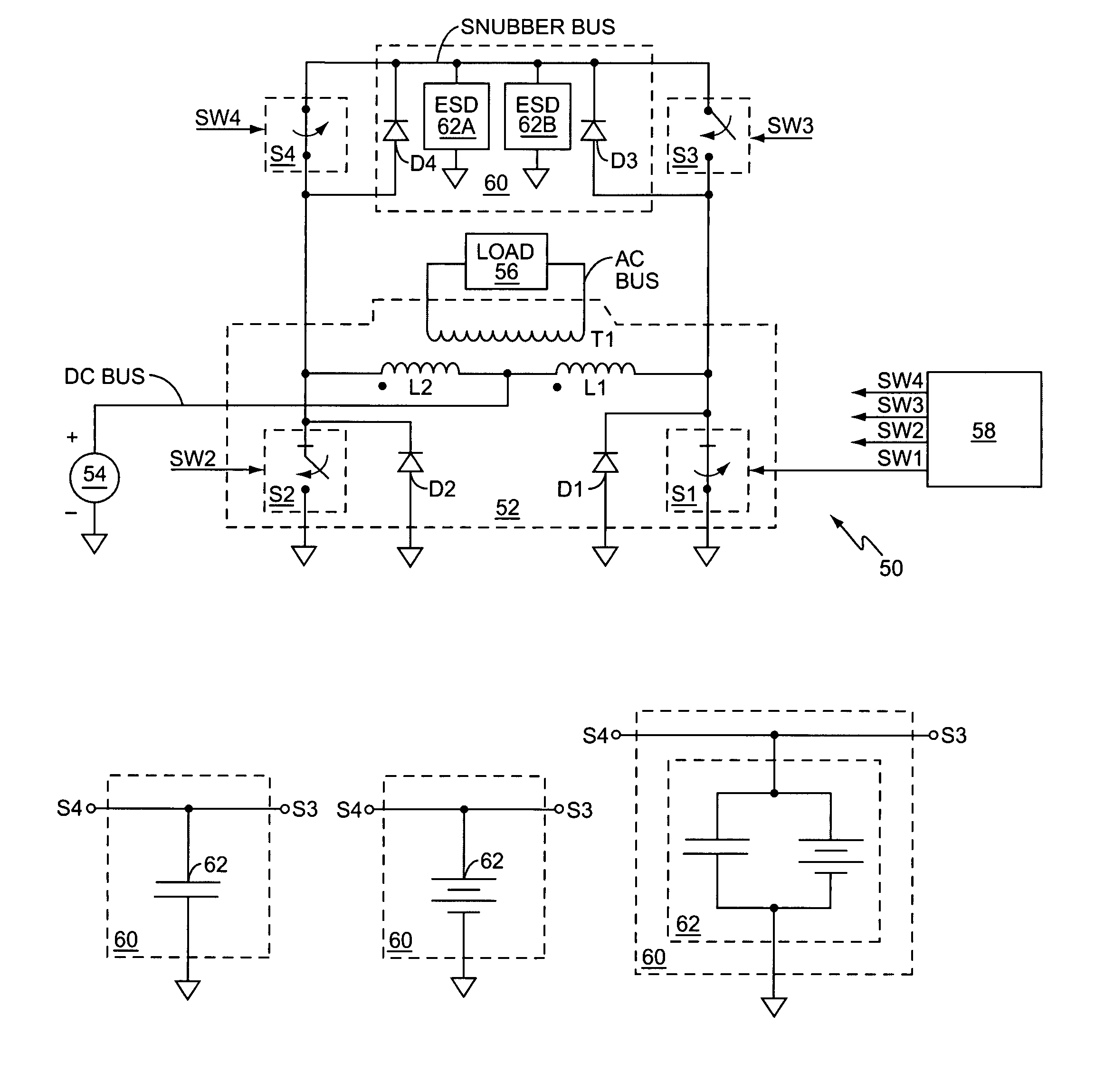
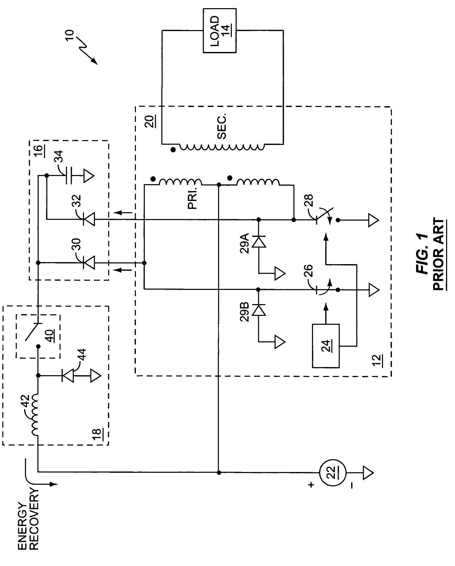
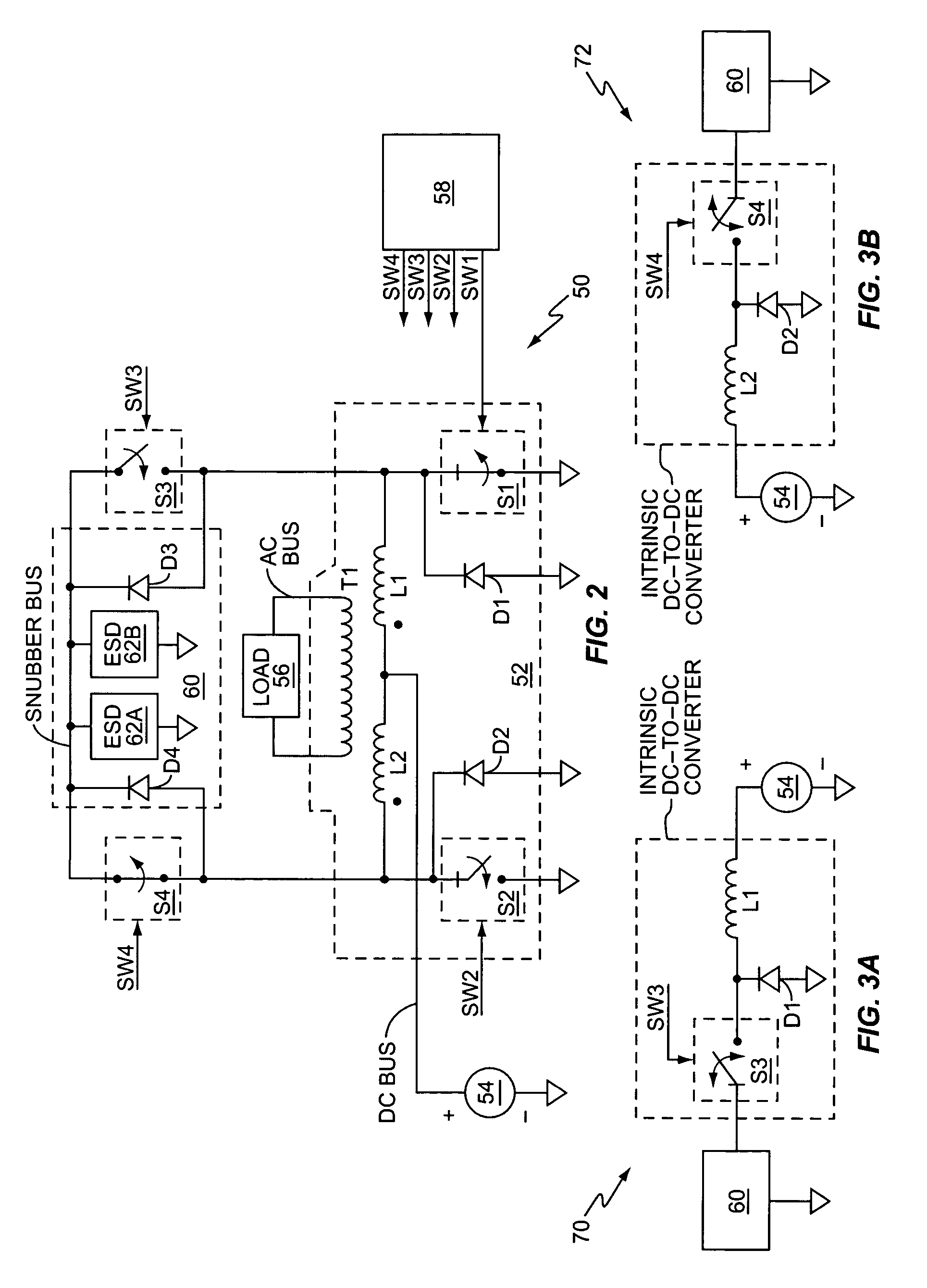
[0028]FIG. 1 is a diagram of a conventional power inverter 10 comprising a push-pull inverter circuit 12 coupled to a load 14, a snubber circuit 16, and a buck converter circuit 18 configured to enhance inverter efficiency by recovering a portion of the energy stored in the snubber circuit 16. In operation, an inverter transformer 20 is used to convert DC power from a DC supply 22 based on a switching controller 24 opening and closing main power switches 26 and 28.

[0029]As those skilled in the art will appreciate, an AC waveform of a desired voltage can be set up on the secondary winding of transformer 20 based on alternately switching power switches 26 and 28 on and off according to a desired duty cycle. The commutation of primary winding current from first and second halves of the center-tapped primary winding by operation of switches 26 and 28 is supported by the use of free-wheeling diodes 29A and 29B, as is understood by those skilled in the art.

[0030]The generation of voltage ...


PUM


Abstract

A power inverter comprises a push-pull inverter circuit that includes a transformer having a primary winding coupled to a DC bus and a secondary winding coupled to an AC bus, main power switches coupling each end of the primary winding to a DC return, and one or more supplemental power switches coupling at least one end of the primary winding to a snubber bus. The supplemental switch at a given end of the primary winding forms a buck-mode converter in combination with the primary winding and the associated free-wheeling diode at that end of the primary winding, and can be controlled by a switching controller to effect energy transfer between the snubber bus and DC bus. The switching controller can be configured to control power flow between the DC, AC, and snubber buses by controlling the common-mode and differential-mode voltages of the primary winding via main / supplemental power switch control.

Description

BACKGROUND OF THE INVENTION[0001]The present invention generally relates to power conversion, and particularly relates to push-pull inverter circuits with snubber-based energy recovery.[0002]Push-pull inverter circuits are commonly used in power conversion applications, such as in DC-to-AC power inverters. In terms of construction, such inverter circuits typically comprise a transformer with a switched primary winding having its center tap coupled to a source of DC power. Each end of the primary winding is coupled to a DC return through a switch, and output AC power is provided by the transformer's secondary winding based on alternately turning on one or the other switch at a desired frequency. Output voltage variations are achieved by varying the relative conduction intervals of the two switches, and the switching control signals can be generated as Pulse Width Modulation (PWM) signals of essentially any desired resolution.[0003]As a general rule, push-pull inverter circuits must b...

Claims


Application Information

Patent Timeline
Patent Type & Authority Patents(United States)
IPC IPC(8): H02H7/122
CPCH02M3/337
Inventor LIPTAK, JULIUS MICHAELKOCHER, MARK JOHNMACKENZIE, IV, JOHN KENNETH
Owner SQUARE D CO
Why Eureka
Try Eureka