Method and structure for double dose gate in a JFET

a junction field effect transistor and gate technology, applied in the field of junction field effect transistors, can solve the problem of limiting the diffusion path of the implanted, and achieve the effects of reducing cgs and cgd, increasing flexibility in control, and improving performan

Inactive Publication Date: 2006-02-07
POWER INTEGRATIONS INC
View PDF2 Cites 17 Cited by
  • Summary
  • Abstract
  • Description
  • Claims
  • Application Information

AI Technical Summary

Benefits of technology

[0011]Thus, a need exists for a JFET with minimal parasitic capacitances Cgs and Cgd. There is also a need for method for producing an optimal JFET structure that is compatible with the process flow used for logic integrated circuits. Additionally there is a need for increased flexibility in the control of the lateral doping profile in a gate structure.
[0012]Accordingly, embodiments of the present invention include a JFET structure that has reduced Cgs and Cgd and provides improved performance at high frequencies and greater power efficiency. Another aspect of the invention is a fabrication method that is readily integrated with a conventional process flow for logic integrated circuits. These and other objects and advantages of the present invention and others not specifically recited above will be described in more detail herein.
[0013]In an embodiment of the present invention, a gate definition spacer is formed on the wall of an etched trench to establish the lateral extent of an implanted gate region for a JFET. After implant, the gate is annealed. In addition to controlling the final junction geometry and thereby reducing the junction capacitance by establishing the lateral extent of the implanted gate region, the gate definition spacer also limits the available diffusion paths for the implanted dopant species during anneal. The net result is that the interfacial area between the gate and source and gate and drain are reduced, thereby reducing the associated parasitic capacitances Cgs and Cgd.
[0014]In another embodiment of the present invention, a gate region is formed by implanting and annealing. After annealing, a portion of the gate structure that is not directly adjacent to the channel is removed, thereby decreasing the parasitic capacitance Cgd between the gate and drain.
[0015]In a further embodiment of the present invention two ion implant steps are performed over different but overlapping volumes in order to provide an additional degree of flexibility in controlling doping profile of the gate region. By using a “double dose” process comprising a low dose for the first implant over a larger volume followed by a high dose implant over a smaller volume, a graded junction is obtained.

Problems solved by technology

In addition to controlling the final junction geometry and thereby reducing the junction capacitance by establishing the lateral extent of the implanted gate region, the gate definition spacer also limits the available diffusion paths for the implanted dopant species during anneal.

Method used


Image

  • Method and structure for double dose gate in a JFET
  • Method and structure for double dose gate in a JFET
  • Method and structure for double dose gate in a JFET

Examples


Embodiment Construction

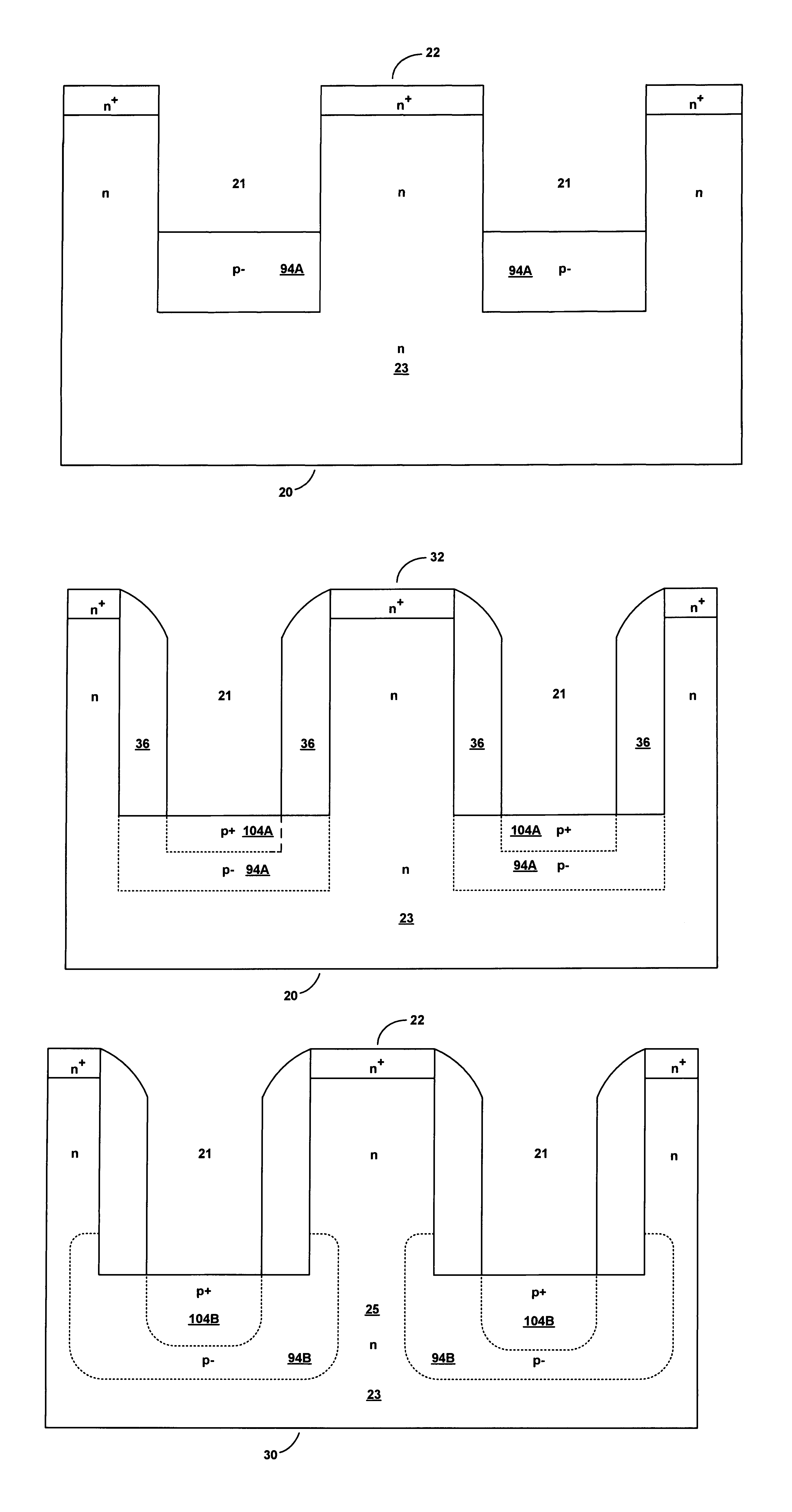
[0035]In the following detailed description of the present invention, a junction field effect transistor (JFET) structure with reduced parasitic capacitances and a method for fabricating the structure; numerous specific details are set forth in order to provide a thorough understanding of the present invention. However, it will be obvious to one skilled in the art that the present invention may be practiced without these specific details. In other instances well known methods involving photolithography, deposition and etch, etc., and well known structures such as ohmic contacts and barrier metallization, etc., have not been described in detail so as not to unnecessarily obscure aspects of the present invention.

[0036]U.S. Pat. No. 6,251,716 entitled “JFET Structure and Manufacture Method for Low On-Resistance and Low Voltage Application,” issued Jun. 26, 2001, and assigned to the assignee of the present invention, is hereby incorporated herein by reference.

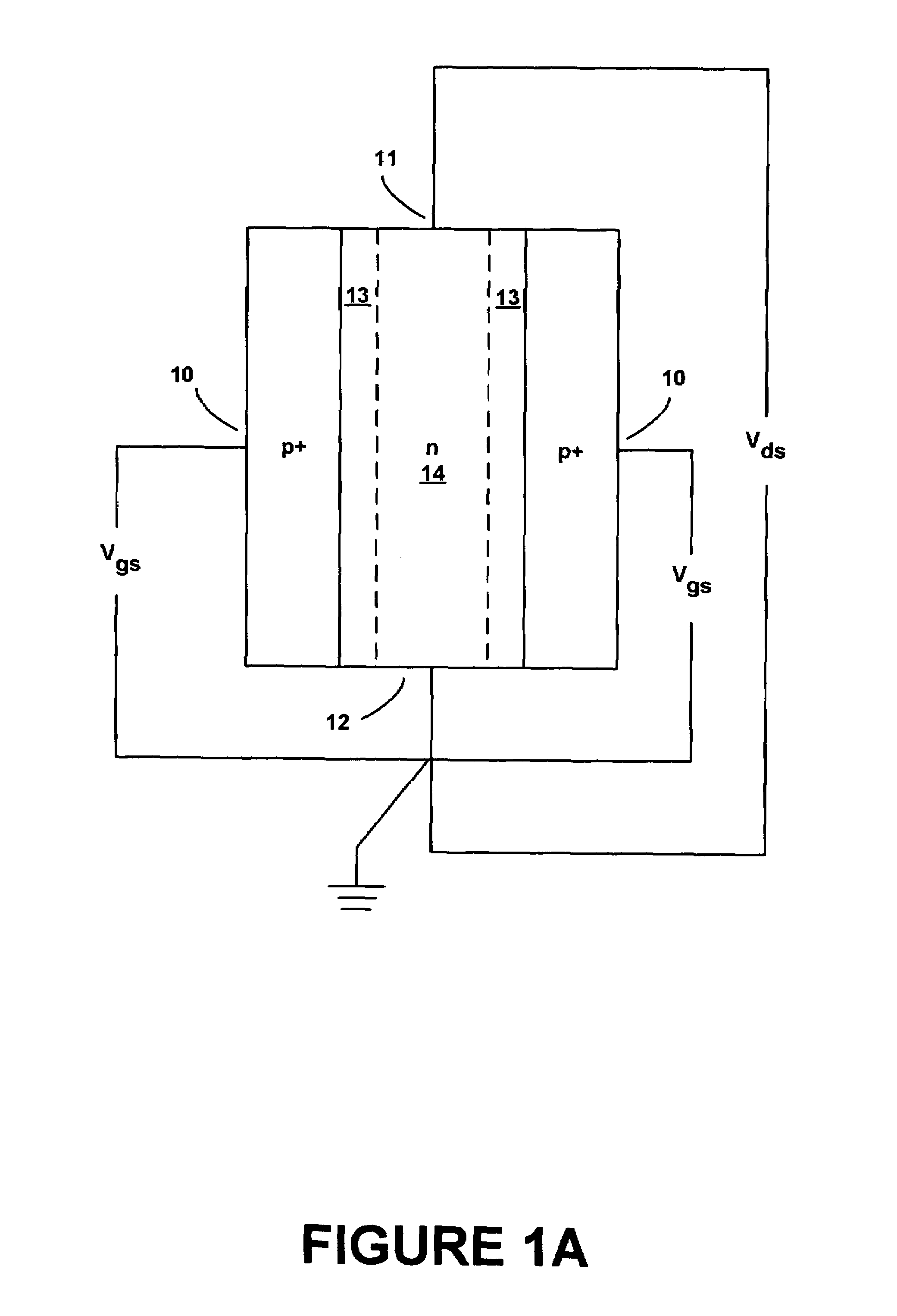
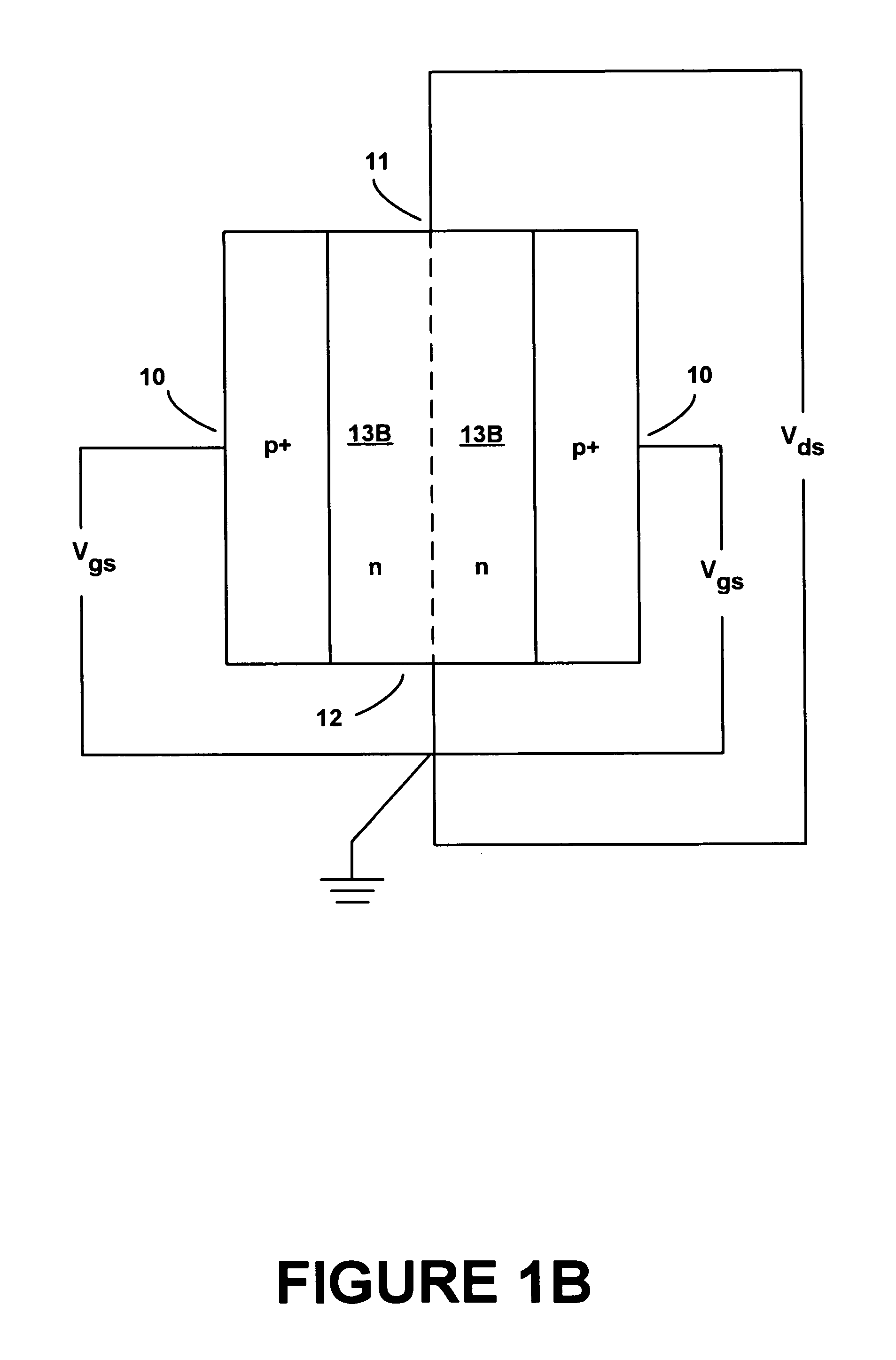
[0037]FIG. 1A shows a gener...


PUM


Abstract

A method for fabricating a junction field effect transistor (JFET) with a double dose gate structure. A trench is etched in the surface of a semiconductor substrate, followed by a low dose implant to form a first gate region. An anneal may or may not be performed after the low dose implant. A gate definition spacer is then formed on the wall the trench to establish the lateral extent of a second, high dose implant gate region. After the second implant, the gate is annealed. The double dose gate structure produced by the superposition of two different and overlapping regions provides an additional degree of flexibility in determining the ultimate gate region doping profile. A further step comprises using the gate definition spacer to define the walls of a second etched trench that is used to remove a portion of the p-n junction, thereby further reducing the junction capacitance.

Description

[0001]This application is a DIV of Ser. No. 10 / 191,030 Jul. 2, 2002 U.S. Pat. No. 6,777,722.FIELD OF THE INVENTION[0002]Embodiments of the present invention relate to the field of junction field effect transistors (JFETs). More particularly, embodiments of the present invention relate to a reduction in the input capacitance of JFETs.BACKGROUND ART[0003]Junction field effect transistors (JFETs) are majority carrier devices that conduct current through a channel that is controlled by the application of a voltage to a p-n junction. JFETs may be constructed as p-channel or n-channel and may be operated as enhancement mode devices or depletion mode devices.[0004]The most common JFET type is the depletion mode type. The depletion mode device is a normally “on” device that is turned off by reverse biasing the p-n junction so that pinch-off occurs in the conduction channel. P-channel depletion mode devices are turned off by the application of a positive voltage between the gate and source (...

Claims


Application Information

Patent Timeline
Patent Type & Authority Patents(United States)
IPC IPC(8): H01L21/338H01L21/337H01L29/10H01L29/808
CPCH01L29/1066H01L29/8083H01L29/66909
Inventor YU, HO-YUANLIVA, VALENTINO L.PEGLER, PETE
Owner POWER INTEGRATIONS INC
Why Eureka
Try Eureka