Synthetic pattern exchange configuration for side reading reduction
a technology of synthetic pattern and side reading, applied in the field of synthetic pattern exchange configuration, can solve the problems of reducing the sensitivity of the sensor and undesirable level of side reading, and achieve the effect of convenient fabrication, optimal thickness ratio, and magnetically stable results
- Summary
- Abstract
- Description
- Claims
- Application Information
AI Technical Summary
Benefits of technology
Problems solved by technology
Method used
Image
Examples
first embodiment
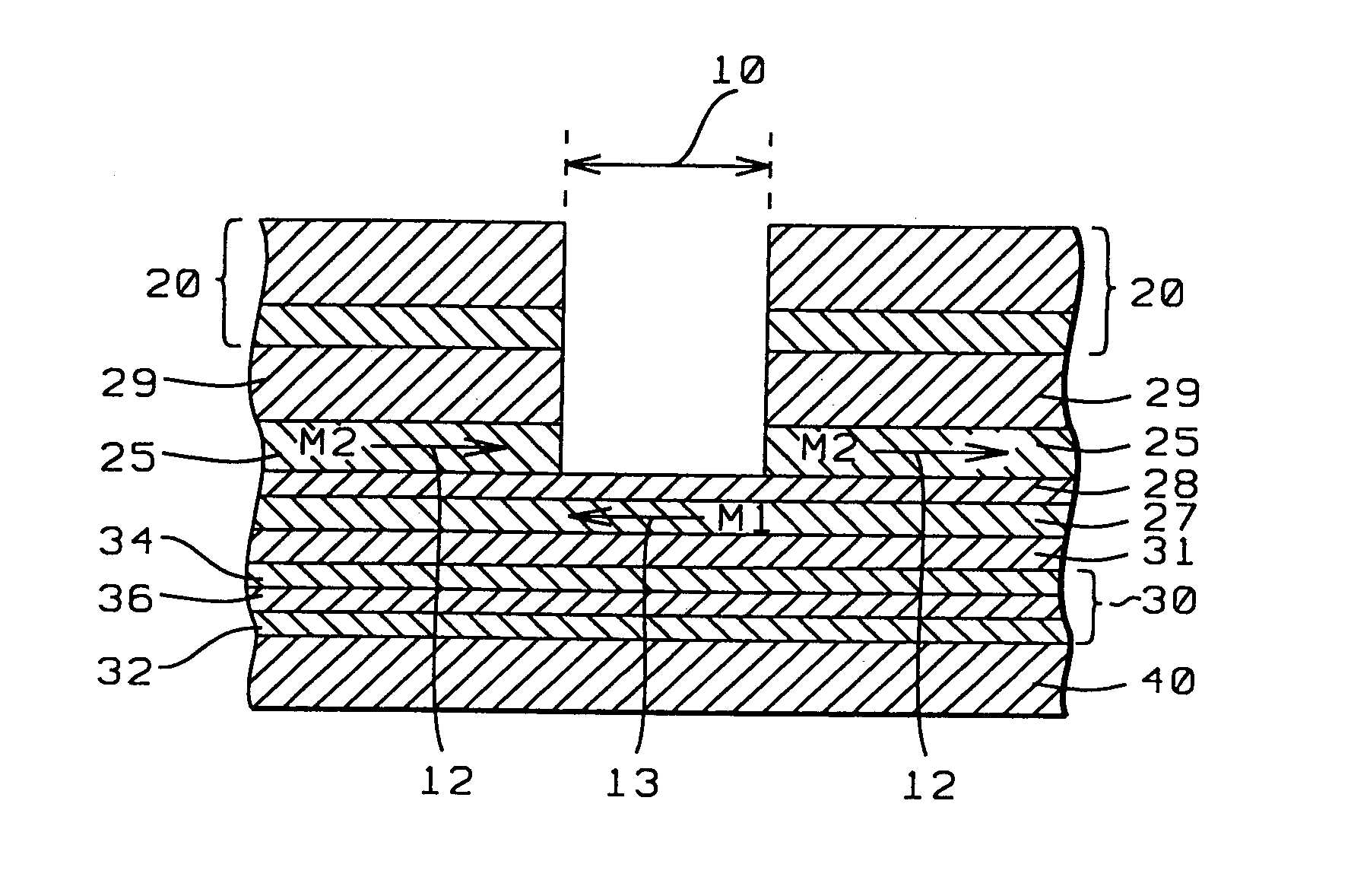
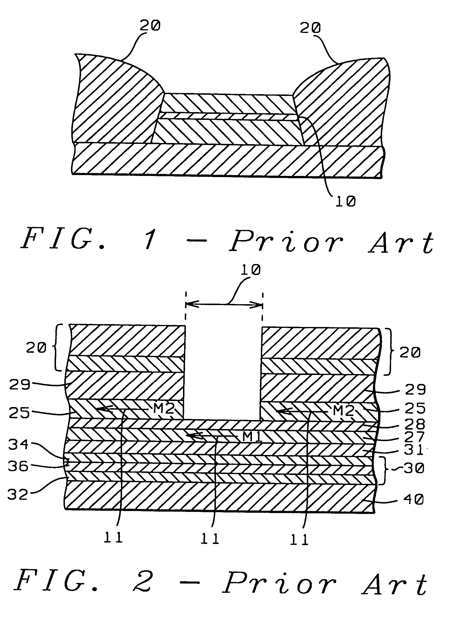
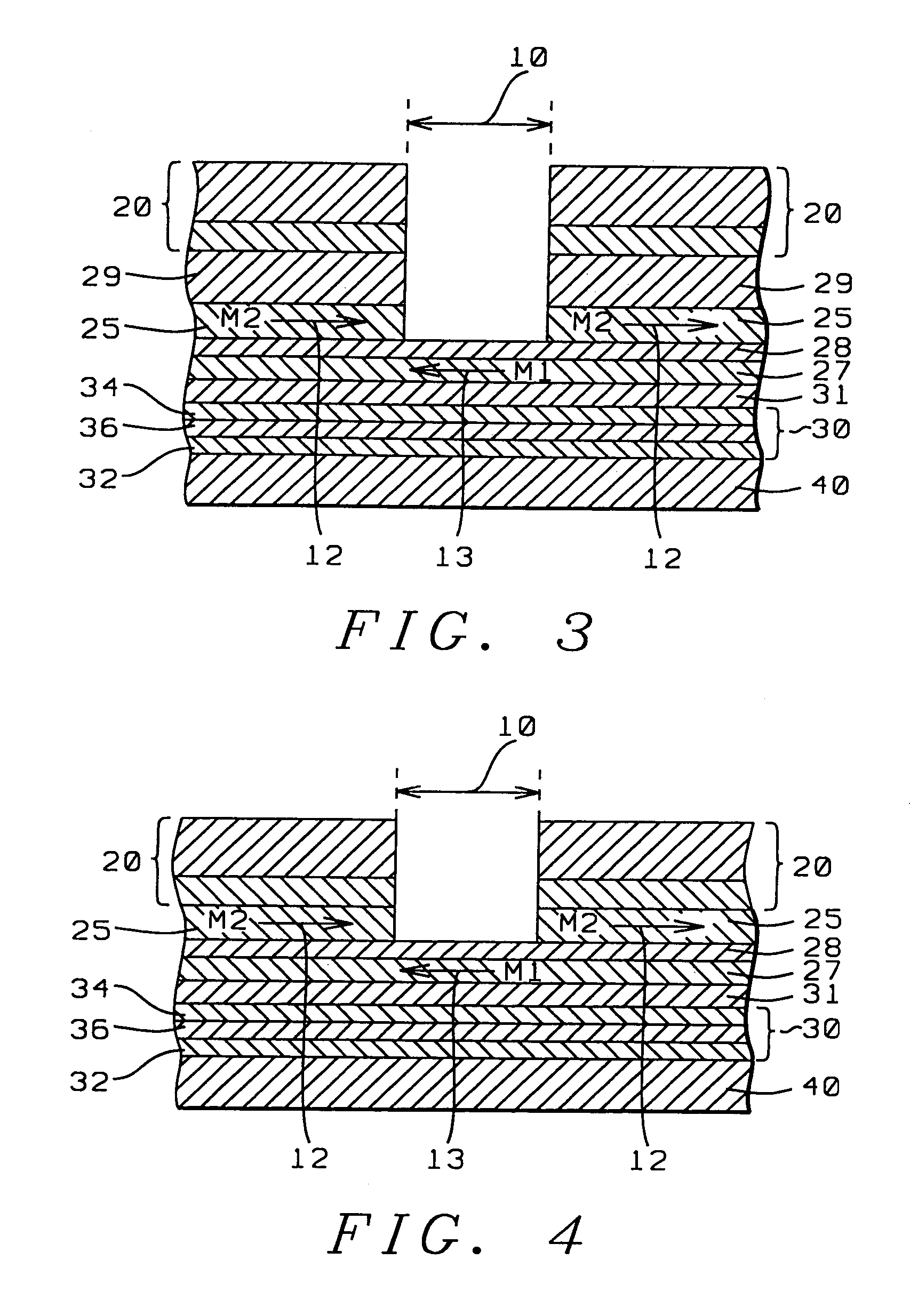
[0036]Referring next to FIG. 3, there is shown a schematic cross-sectional view of the ABS surface of a patterned synthetic exchange longitudinally biased GMR sensor whose structure and method of fabrication are fully described in related patent application HT01-0361038 and which is fully incorporated herein by reference. This structure is similar in many respects to the direct exchange configuration of FIG. 2. except for the antiparallel directions of the F2 and F1 magnetic moments M2 (12), M1 (13). It is this configuration of FIG. 3 which, when properly designed and optimized in accord with the simulations of the present invention, constitutes the present invention. The following dimensions, however, are those disclosed in HT01-036 / 038 and are not in accord with the present invention. The physical trackwidth (10) of this configuration is approximately 0.1 microns and is defined by the width of the region between the leads (20) and patterned biasing (25) layers (F2). Typically, F2 ...
second embodiment
The numbers are thicknesses in angstroms, the “X” in CoFe represents the variable simulation thickness of the F2 layer that is used to distinguish the four graphs, X=15 angstroms, 25 angstroms, 28 angstroms and 35 angstroms. FM, representing a ferromagnetic layer, is used to simplify the simulation. Referring to the figure, it can be seen that with the increase in F2 thickness from 15 to 35 angstroms, the F1 rotation angle under low field first decreases with F2 thickness and reaches a minimum for F2=28 angstroms, then increases again with F2 thickness. For each fixed value of F1, as well as values of Jex and Js, there is an optimum thickness of F2, so different configurations will generally require different optimizations. In the simulated structure above, Js=0.25 erg / cm2 and Jex=0.1 erg / cm2. It is to be noted that the IrMn layer would be absent in FIG. 4
[0042]Referring next to FIG. 6, there is shown a graph relating F2 thickness to the relative sensor signal produced by only the l...
PUM
| Property | Measurement | Unit |
|---|---|---|
| thickness | aaaaa | aaaaa |
| thickness | aaaaa | aaaaa |
| thickness | aaaaa | aaaaa |
Abstract
Description
Claims
Application Information


