Semiconductor device and method of manufacture thereof, circuit board, and electronic instrument

a semiconductor device and semiconductor technology, applied in the direction of solid-state devices, semiconductor/solid-state device details, printed circuit structure associations, etc., can solve the problems of reducing the yield of the semiconductor device when the semiconductor device is mounted, the placement of the semiconductor device, and the use of expensive circuit boards fine interconnecting lines. to achieve the effect of convenient mounting on the circuit board

Inactive Publication Date: 2007-02-27
ADVANCED INTERCONNECT SYST LTD
View PDF25 Cites 19 Cited by
  • Summary
  • Abstract
  • Description
  • Claims
  • Application Information

AI Technical Summary

Benefits of technology

The present invention allows for the easy manufacturing of a semiconductor device that can be easily mounted on a circuit board.

Problems solved by technology

The technical problem addressed in this patent is the difficulty in efficiently utilizing the area of the circuit board when mounting semiconductor devices on it, due to the fine pitch of the connector terminals used for connecting the semiconductor device to the circuit board. This can result in a reduction in yield when mounting the semiconductor device and an increase in the area of the circuit board occupied by the semiconductor device.

Method used


Image

  • Semiconductor device and method of manufacture thereof, circuit board, and electronic instrument
  • Semiconductor device and method of manufacture thereof, circuit board, and electronic instrument
  • Semiconductor device and method of manufacture thereof, circuit board, and electronic instrument

Examples


first embodiment

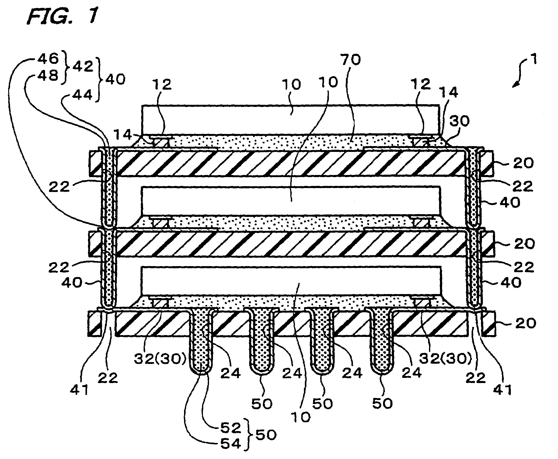
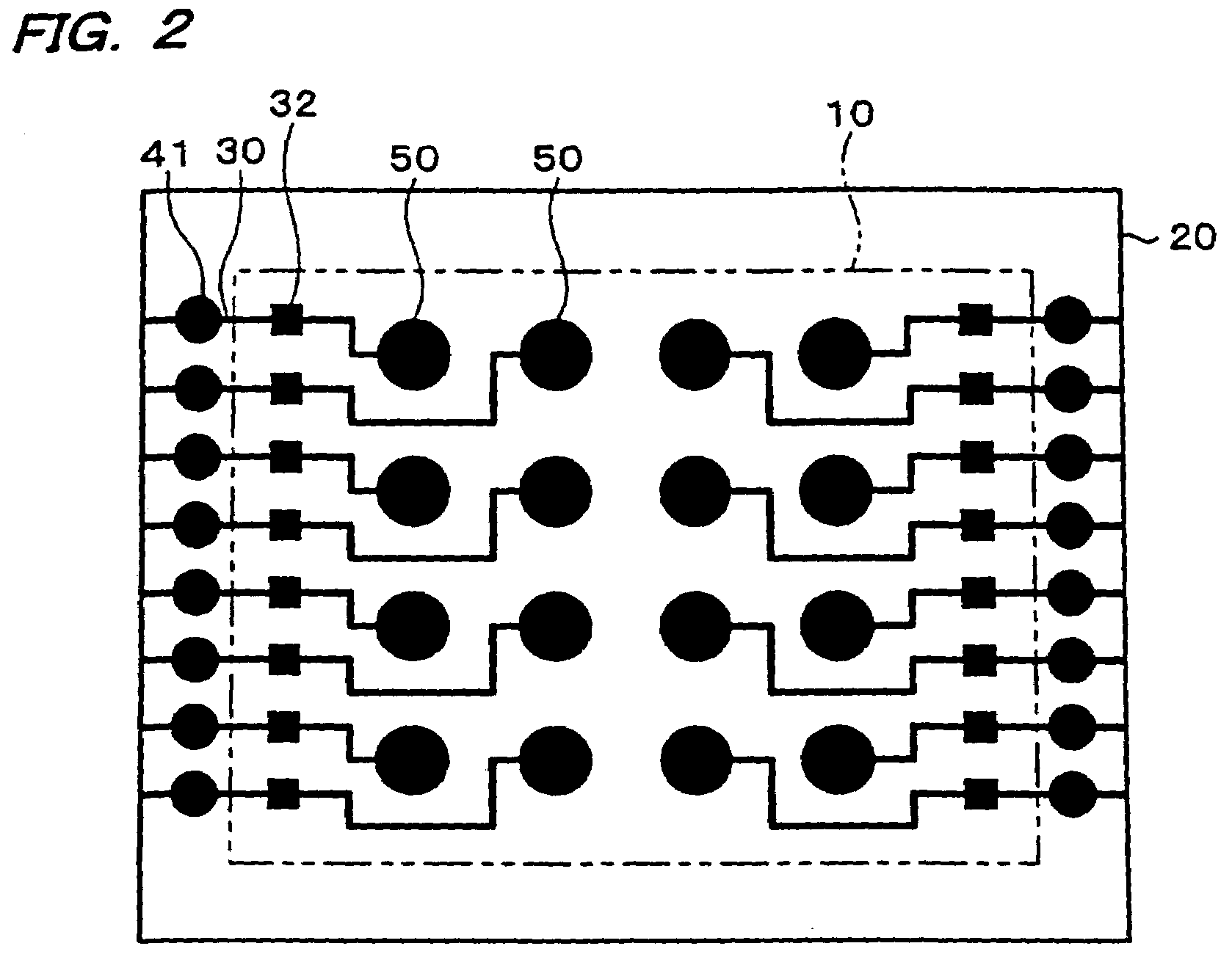
[0073]FIG. 1 to FIG. 3 show this embodiment of a semiconductor device. FIG. 1 is a cross-section of the semiconductor device, and FIG. 2 is a plan view of a lowest substrate 20. FIG. 3 is a sectional view of a variant of this embodiment of the semiconductor device.

[0074]A semiconductor device 1 shown in FIG. 1 comprises a plurality of semiconductor chips 10 and a plurality of substrates 20. Each semiconductor chip 10 is mounted on a substrate 20. The semiconductor device 1 is formed by respective substrates 20 being laminated, and upper and lower semiconductor chips 10 electrically connected. Such a semiconductor device 1 can be termed a semiconductor device of stacked construction.

[0075]The outline of the semiconductor chip 10 is commonly rectangular. The semiconductor chip 10 has a plurality of electrodes 12. The electrodes 12 are electrodes of the integrated circuit formed on the semiconductor chip 10. The electrodes 12 may be formed on the surface of the semiconductor chip 10 ha...

second embodiment

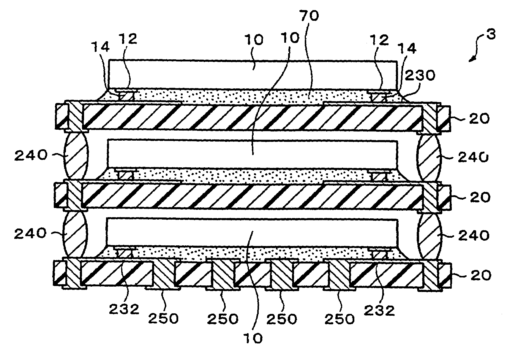
[0120]FIG. 4 is a sectional view of this embodiment of the semiconductor device. This embodiment differs from the above described example in the form of an interconnecting pattern 230 formed on the substrate 20. The interconnecting pattern 230 comprises a plurality of interconnecting lines and electrical connections 232.

[0121]As shown in FIG. 4, the interconnecting pattern 230 is formed on both surfaces of the substrate 20. As shown in the drawing, by means of a plurality of through holes in the substrate 20, the interconnecting pattern 230 may be formed with both surfaces electrically connected. The through holes, as shown in the drawing, may be filled with the material of the interconnecting pattern 230. Alternatively, the through holes may be formed with through holes in a central portion, and may be vertically electrically conducting on the periphery formed by the inner wall. It should be noted that the interconnecting pattern 230 may be formed by providing a conducting material...


PUM


Abstract

A semiconductor device includes a plurality of semiconductor chips; and a plurality of substrates, each of the substrates having one of the semiconductor chips mounted thereon. The substrates are stacked each other. The upper and lower ones of the semiconductor chips mounted on a pair of the stacked substrates are electrically connected through first terminals provided in a region outside the region in which one of the semiconductor chips is mounted in each of the substrates. The lowest one of the substrates has second terminals provided in its region closer to its center than its region in which the first terminals are provided, the second terminals electrically connected to one of the semiconductor chips. A pitch of adjacent two of the second terminals is wider than a pitch of adjacent two of the first terminals.

Description


Claims


Application Information

Patent Timeline
Owner ADVANCED INTERCONNECT SYST LTD
Why Eureka
Try Eureka