Method and apparatus for enhancing signal routability

Inactive Publication Date: 2007-02-27
ALTERA CORP
View PDF3 Cites 3 Cited by
  • Summary
  • Abstract
  • Description
  • Claims
  • Application Information

AI Technical Summary

Benefits of technology

[0009]In one embodiment, a method for enhancing signal routability within an integrated circuit is provided. The method initiates with examining an outer edge of a sequence of logical array blocks. The method includes identifying an undriven routing wire in a vicinity of the outer edge. An underutilized driver proximate to the undriven routing wire is also identified. Then, the underutilized driver is coupled to the undriven routing wire.

Problems solved by technology

Similarly, some of the wires that drive towards the right edge of the chip are relatively short because of the truncation effects due to the proximity to the edge of the chip.
However, due to the short length of the wires the driver / wire configuration can only communicate with three or fewer LABs, or a single I / O block.

Method used


Image

  • Method and apparatus for enhancing signal routability
  • Method and apparatus for enhancing signal routability
  • Method and apparatus for enhancing signal routability

Examples


Embodiment Construction

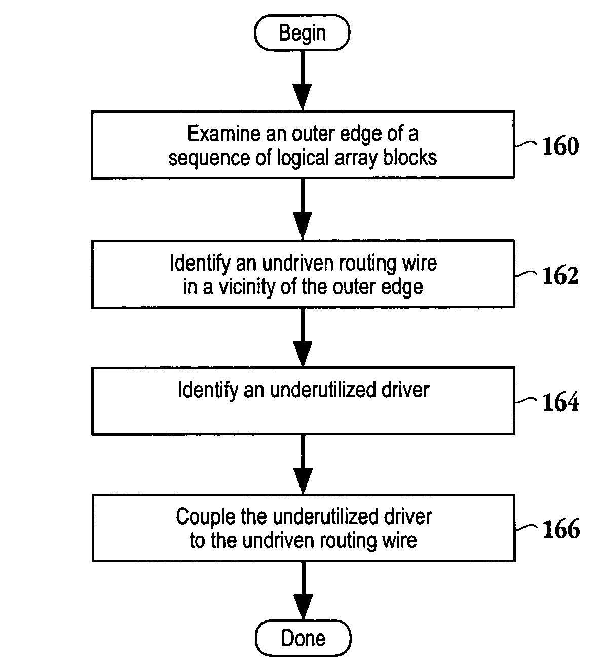
[0022]An invention is described for an apparatus and method for enhancing signal routability at the edge of a chip having a segmented routing scheme. It will be obvious, however, to one skilled in the art, that the present invention may be practiced without some or all of these specific details. In other instances, well known process operations have not been described in detail in order not to unnecessarily obscure the present invention.

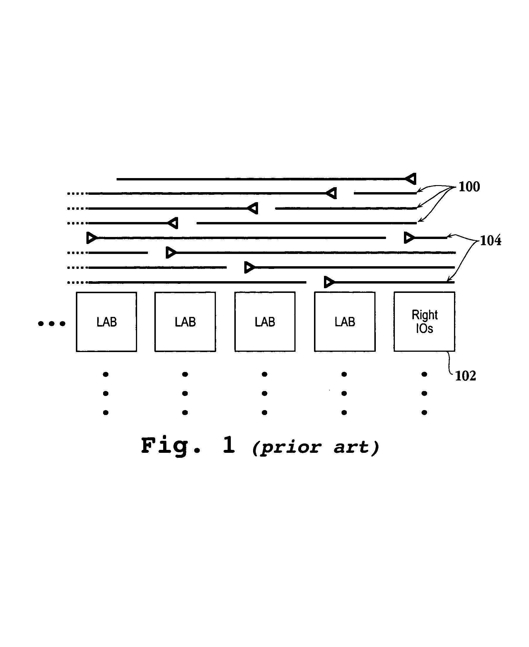
[0023]A programmable logic device is a digital, user-configurable integrated circuit used to implement a custom logic function. For the purposes of this description, the term PLD encompasses any digital logic circuit configured by the end-user, and includes a programmable logic array, a field programmable date array, and an erasable and complex PLD. The embodiments described herein provide for the enhancement of signal routing in a segmented / staggered wiring scheme, e.g., an H4 wiring scheme. The implementation of the wiring schemes described herein ...


PUM


Abstract

A method for enhancing signal routability within an integrated circuit is provided. The method initiates with examining an outer edge of a sequence of logical array blocks. The method includes identifying an undriven routing wire in a vicinity of the outer edge. An underutilized driver proximate to the undriven routing wire is also identified. Then, the underutilized driver is coupled to the undriven routing wire. A computer readable medium and an integrated circuit are also provided.

Description

BACKGROUND OF THE INVENTION[0001]1. Field of the Invention[0002]This invention relates generally to Integrated Circuits and, in particular, to routing wires within a programmable logic device (PLD).[0003]2. Description of the Related Art[0004]The basic building block of the PLD is a logic element that is capable of performing limited logic functions on a number of input variables. The logic element is typically equipped with circuitry to programmably implement the “sum of products” logic, as well as one or more registers to implement sequential logic. Conventional PLDs combine together large numbers of such logic elements through an array of programmable interconnections to facilitate implementation of complex logic functions. PLDs have found particularly wide application as a result of their combined low up-front cost and versatility to the user.[0005]A variety of PLD architectural approaches arranging the interconnect array and logic elements have been developed to optimize logic ...

Claims


Application Information

Patent Timeline
IPC IPC(8): G06F17/50
CPCG06F17/5077G06F30/394
Inventor LEVENTIS, PAULCASHMAN, DAVID
Owner ALTERA CORP
Why Eureka
Try Eureka