Simplified Substrates for Semiconductor Devices in Package-on-Package Products

Inactive Publication Date: 2008-10-23
TEXAS INSTR INC
View PDF9 Cites 21 Cited by
  • Summary
  • Abstract
  • Description
  • Claims
  • Application Information

AI Technical Summary

Benefits of technology

[0006]Applicants recognize an existing need for a structure and system for fabricating a semiconductor device based on a low cost, small thickness substrate, wherein the device becomes adaptable to, and versatile in assembling package-on-package products. Specifically, applicants recognize an existing need for dramatically reducing the cost of an insulating substrate by reducing the number of patterned metal layers, while concurrently increasing the pin count for solder ball attachment. Applicants further recognize the need for preserving solder ball coplanarity in spite of more than one solder ball pitch, and for enhancing routability by allowing selective depopulation of solder ball pads.
[0010]Another embodiment of the invention is an insulating sheet-like substrate, which has on one surface a first patterned metal layer with a first and a second array of contact pads. The pads of the first and the second array have a first pitch center-to-center and each pad has a first perimeter. The substrate has on its other surface a second patterned metal layer with a third array of contact pads, which has the first pitch center-to-center and selected contact pads depopulated from the array, and each pad has a third perimeter. Conductive vias between the first and the second metal layers connect aligned contact pads and have a fourth perimeter; the vias are placed in interstitial locations so that the fourth perimeter does not overlap with the first and third perimeters. Routing lines to the contact pads of the third array are distributed in the second metal layer so that required space is provided by the selectively depopulated contact pads. This sacrifice enables a high density of routing line even under the constraint of only two metal layers.

Problems solved by technology

First, the higher product complexity should largely be achieved by shrinking the feature sizes of the chip components while holding the package dimensions constant; preferably, even the packages should shrink.
Second, the increased functional complexity should be paralleled by an equivalent increase in reliability of the product.
Third, the cost per functional unit should drop with each generation of complexity so that the cost of the product with its doubled functionality would increase only slightly.
Recent applications especially for hand-held wireless equipments, combined with ambitious requirements for data volume and high processing speed, place new, stringent constraints on the size and volume of semiconductor components used for these applications.

Method used


Image

  • Simplified Substrates for Semiconductor Devices in Package-on-Package Products
  • Simplified Substrates for Semiconductor Devices in Package-on-Package Products
  • Simplified Substrates for Semiconductor Devices in Package-on-Package Products

Examples


Embodiment Construction

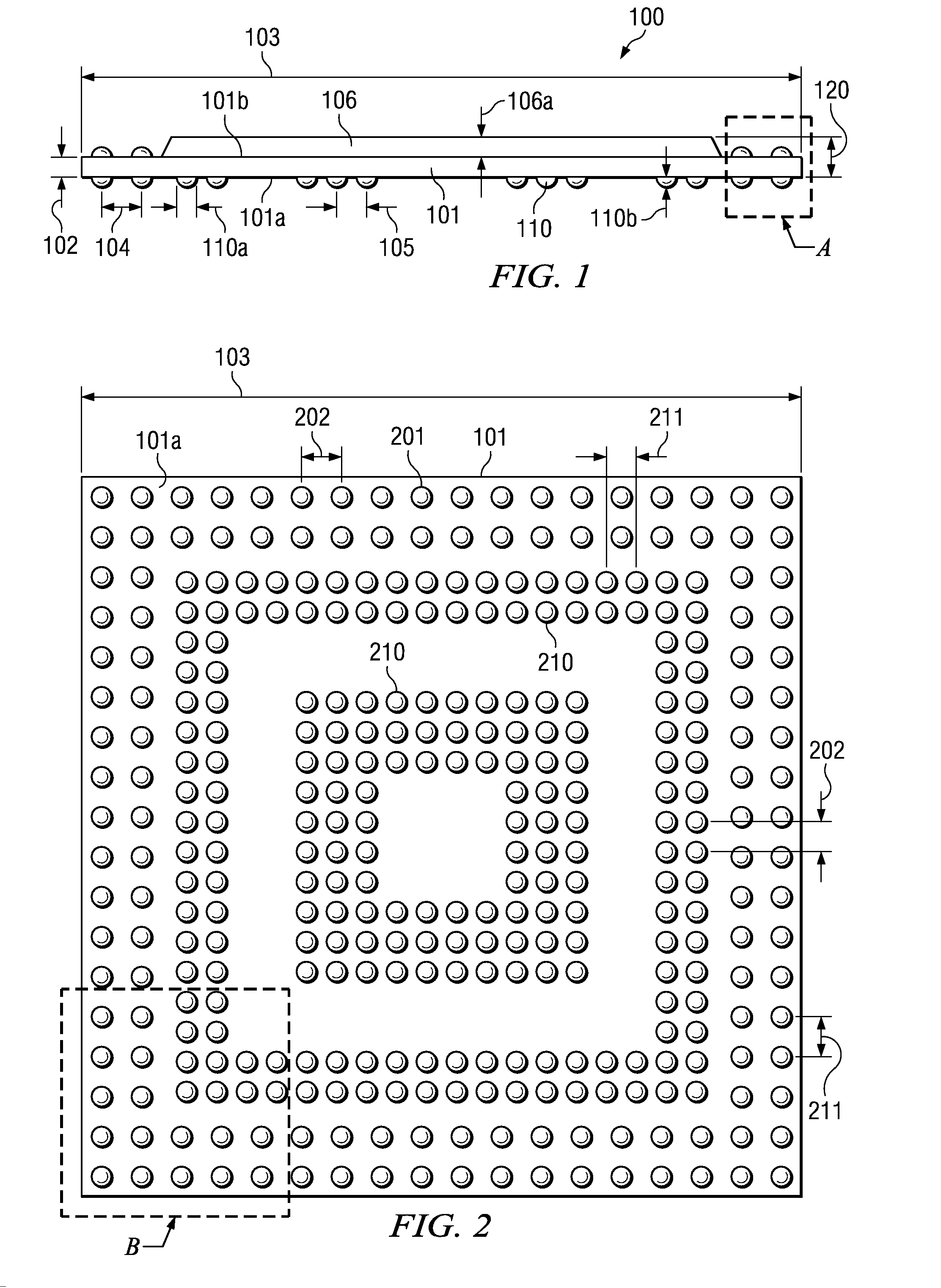
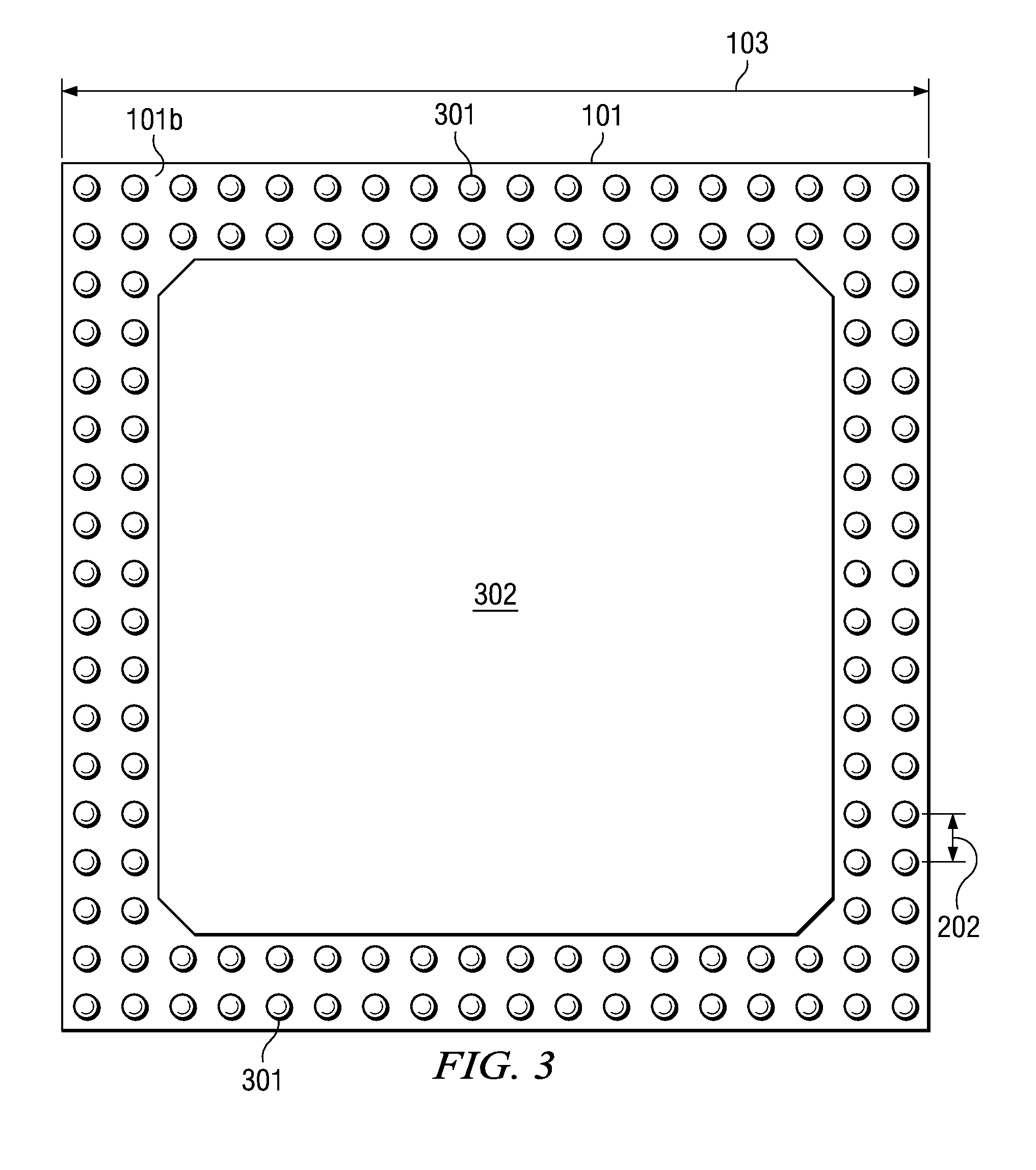
[0022]FIGS. 1, 2 and 3 represent different views of a semiconductor device, generally designated 100, as an embodiment of the invention. The example illustrated is a plastic fine-pitch NF BGA (Ball Grid Array). The device includes sheet-like substrate 101, which is made of insulating materials such as a glass-fiber strengthened epoxy, or a ceramic; in the example of FIG. 1, it has a thickness 102 between about 0.26 and 0.34 mm and a side length of about 12 mm. It should be noted that the invention is applicable to many different sizes and thicknesses of substrates.

[0023]Substrate 101 has a first surface 101a and a second surface 101b. On first surface 101a is a first metal layer and on second surface 101b is a second metal layer (details shown in FIG. 4), preferably copper or a copper alloy. The metal layers are patterned into routing lines (not shown) and contact pads with certain perimeters. The contact pads are arranged in arrays and have pitches 104 and 105, which are discussed ...


PUM


Abstract

An insulating sheet-like substrate (601), which has on one surface (601a) a first patterned metal layer (605) with a first (603a) and a second (603b) array of contact pads. The pads of the first array have a first pitch center-to-center, and each pad has a first perimeter. The pads of the second array have a second pitch center-to-center, and each pad has the first perimeter. The substrate has on its other surface (601b) a second patterned metal layer (606) with a third array (607) of contact pads, which has the first pitch center-to-center, and each pad has a third perimeter. Conductive vias (640) between the first and the second metal layers connect contact pads and have a fourth perimeter; the vias are placed in interstitial locations so that the fourth perimeter does not intersect with the first and third perimeters. Vias in interstitial locations can be provided by disposing the first array and the third array so that the first and third perimeters of respective contact pads are concentrically aligned.

Description

[0001]This application claims priority under 35 U.S.C. § 119 based on Provisional Application Ser. No. 60 / 913,338, filed on Apr. 23, 2007.FIELD OF THE INVENTION[0002]The present invention is related in general to the field of semiconductor devices and processes, and more specifically to structure, layout, and processes of low profile packages for vertically integrated semiconductor systems.DESCRIPTION OF THE RELATED ART[0003]The long-term trend in semiconductor technology to double the functional complexity of its products every 18 months (Moore's rule) has several implicit consequences. First, the higher product complexity should largely be achieved by shrinking the feature sizes of the chip components while holding the package dimensions constant; preferably, even the packages should shrink. Second, the increased functional complexity should be paralleled by an equivalent increase in reliability of the product. Third, the cost per functional unit should drop with each generation o...

Claims


Application Information

Patent Timeline
IPC IPC(8): H01L23/02
CPCH01L23/3128H01L23/49838H01L25/105H01L2224/48091H01L2224/48227H01L2924/01046H01L2924/01079H01L2924/1433H01L2924/15311H01L2924/15331H01L2924/00014H01L24/48H01L2924/14H01L2924/181H01L2924/00H01L2924/00012H01L2224/45099H01L2224/45015H01L2924/207
Inventor HARPER, PETER R.TURNER, JAMES L.LYNE, KEVIN P.WACHTLER, KURT
Owner TEXAS INSTR INC
Why Eureka
Try Eureka