Semiconductor package with enhanced chip groundability and method of fabricating the same

Active Publication Date: 2005-06-07
SILICONWARE PRECISION IND CO LTD
View PDF6 Cites 4 Cited by
  • Summary
  • Abstract
  • Description
  • Claims
  • Application Information

AI Technical Summary

Benefits of technology

[0010]It is therefore an objective of this invention to provide a packaging method for packaging a semiconductor chip with enhanced wire routability for non-grounding wires to make the overall packaging process more simplified to implement.
[0011]It is another objective of this invention to provide a packaging method for packaging a semiconductor chip that can reduce the total number of bond wires required in the wire-bonding process so as to reduce fabrication cost.
[0012]It is still another objective of this invention to provide a packaging method for packaging a semiconductor chip with enhanced wire routability for non-grounding wires, which can provide a shorter grounding path than prior art, so as to reduce the ground bouncing effect to ensure the electrical performance of the package.
[0014]The invention is characterized by providing an electrically-conductive wall on the side surface of each chip for electrically connecting each ground pad on the chip to the grounding plane on the substrate. During subsequent wire-bonding process, since the ground pads on the chip have been already electrically connected to the substrate, the wire-bonding process can be applied only to power and I / O pads. Compared to the prior art, this benefit allows the use of a reduced number of bond wires and also allows the wire routability to be enhanced in wire routability, thereby reducing cost and making the packaging process more simplified to implement. Moreover, the invention allows the ground pads to be connected to the grounding plane on the substrate via a shorter path than prior art, since the length of the electrically-conductive wall is considerably shorter than a grounding wire. This benefit can reduce the ground-bouncing effect and thereby ensure the electrical performance of the package.

Problems solved by technology

One drawback to the conventional electrical connection between a chip and a substrate via bonding wires, however, is that wire routablity would be a problem, particularly in the case of the chip having a great number of densely-arranged ground / power and I / O pads to be electrically connected to the substrate.
Moreover, as the chip is increased in the number of pads, it would require an increased number of bond wires, which are typically made of gold would result in high fabrication cost.
Moreover, by conventional methods, the wire-bonding process would make the total grounding path somewhat lengthy.
Since this grounding path is considerably lengthy, it would result in the so-called ground-bouncing effect that would degrade the electrical performance of the package.
One drawback to this invention, however, is that it would require complex procedural steps to implement.
One drawback to this invention, however, is that the crossed arrangement of the ground ring and the power ring would make the fabrication process more complex and thus difficult to implement.
Moreover, this patent nonetheless requires the use of ground wires for ground connection so that the grounding path is still considerably lengthy that would result in the above-mentioned ground-bouncing effect and thus degrade the electrical performance of the package.

Method used


Image

  • Semiconductor package with enhanced chip groundability and method of fabricating the same
  • Semiconductor package with enhanced chip groundability and method of fabricating the same
  • Semiconductor package with enhanced chip groundability and method of fabricating the same

Examples


Embodiment Construction

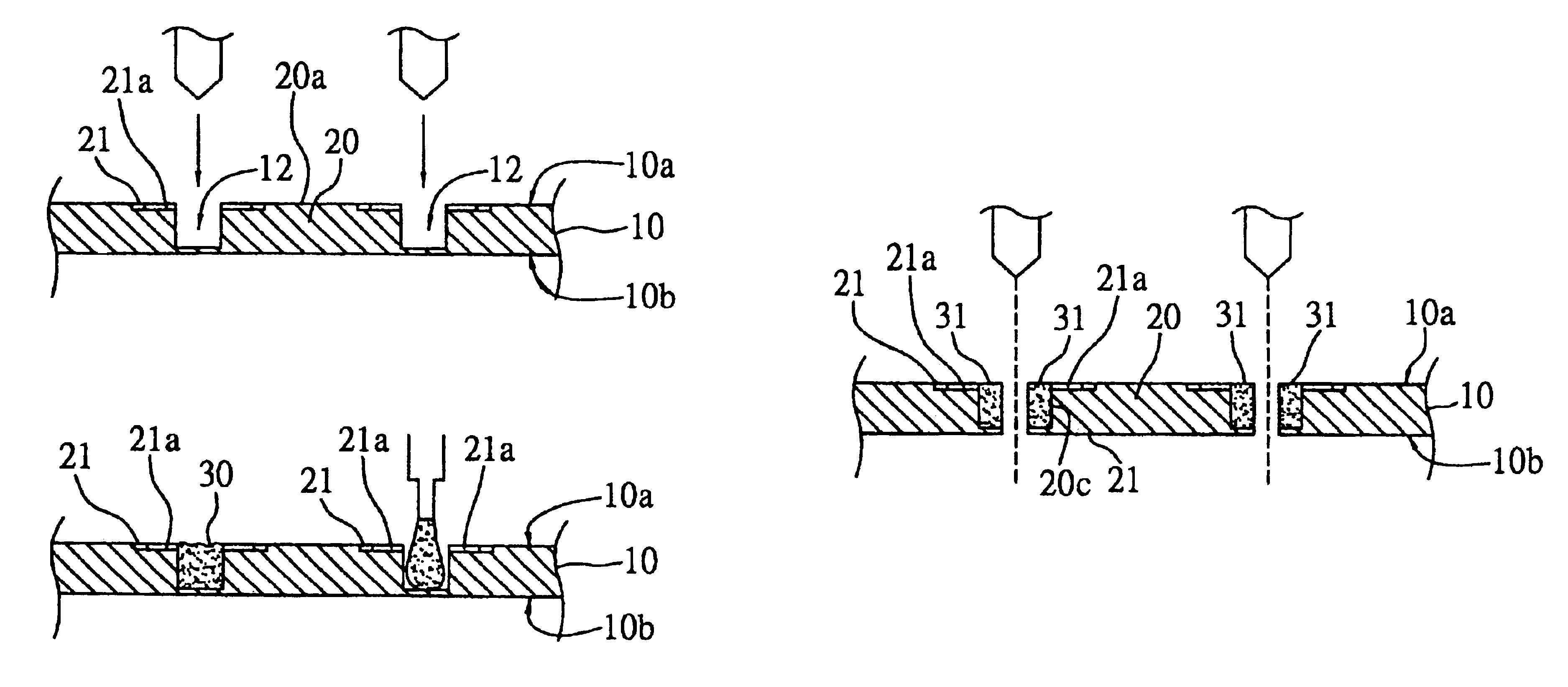
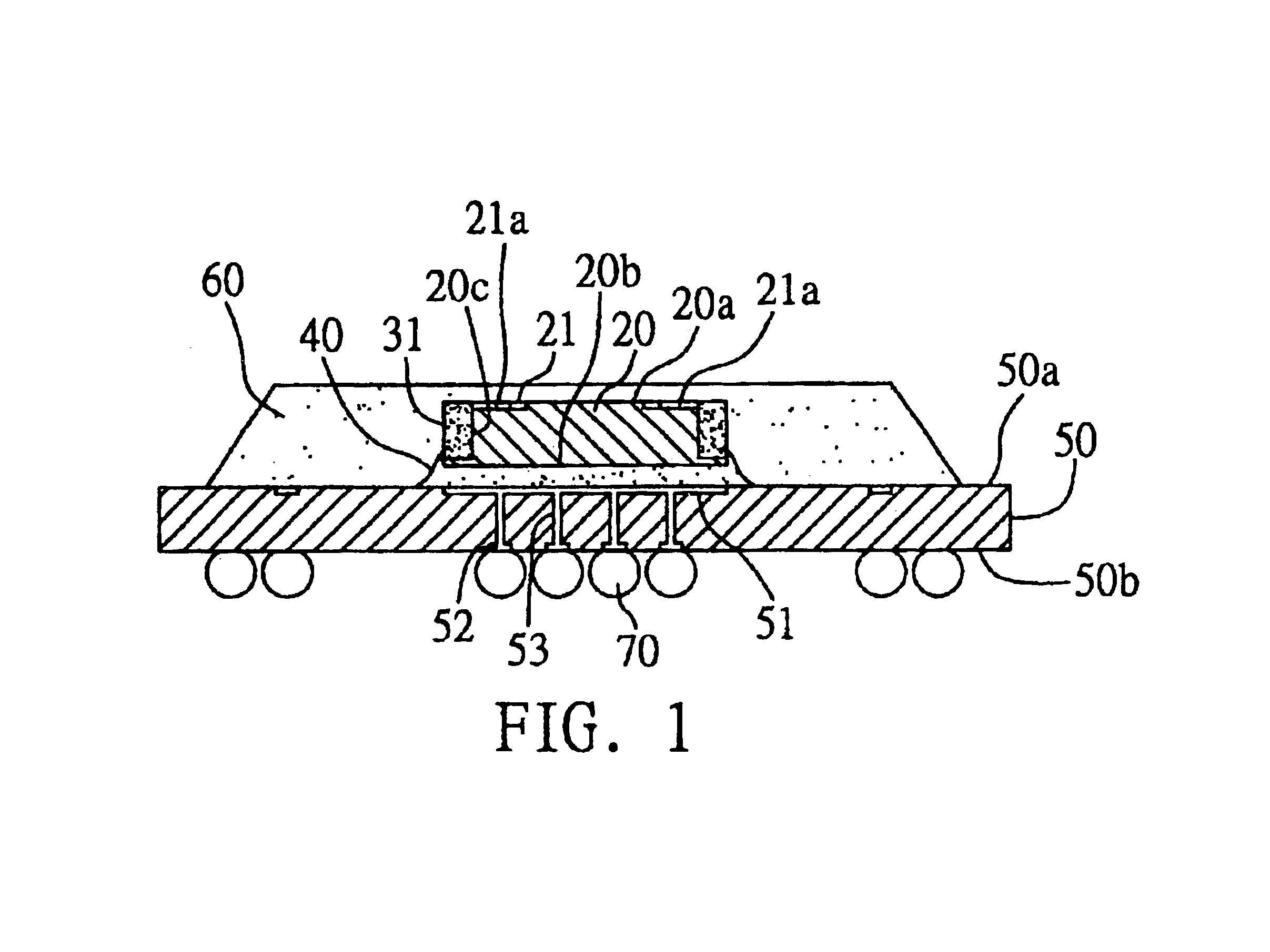
[0023]A preferred embodiment of the semiconductor packaging technology according to the invention is disclosed in full details in the following with reference to FIG. 1 to FIG. 6.

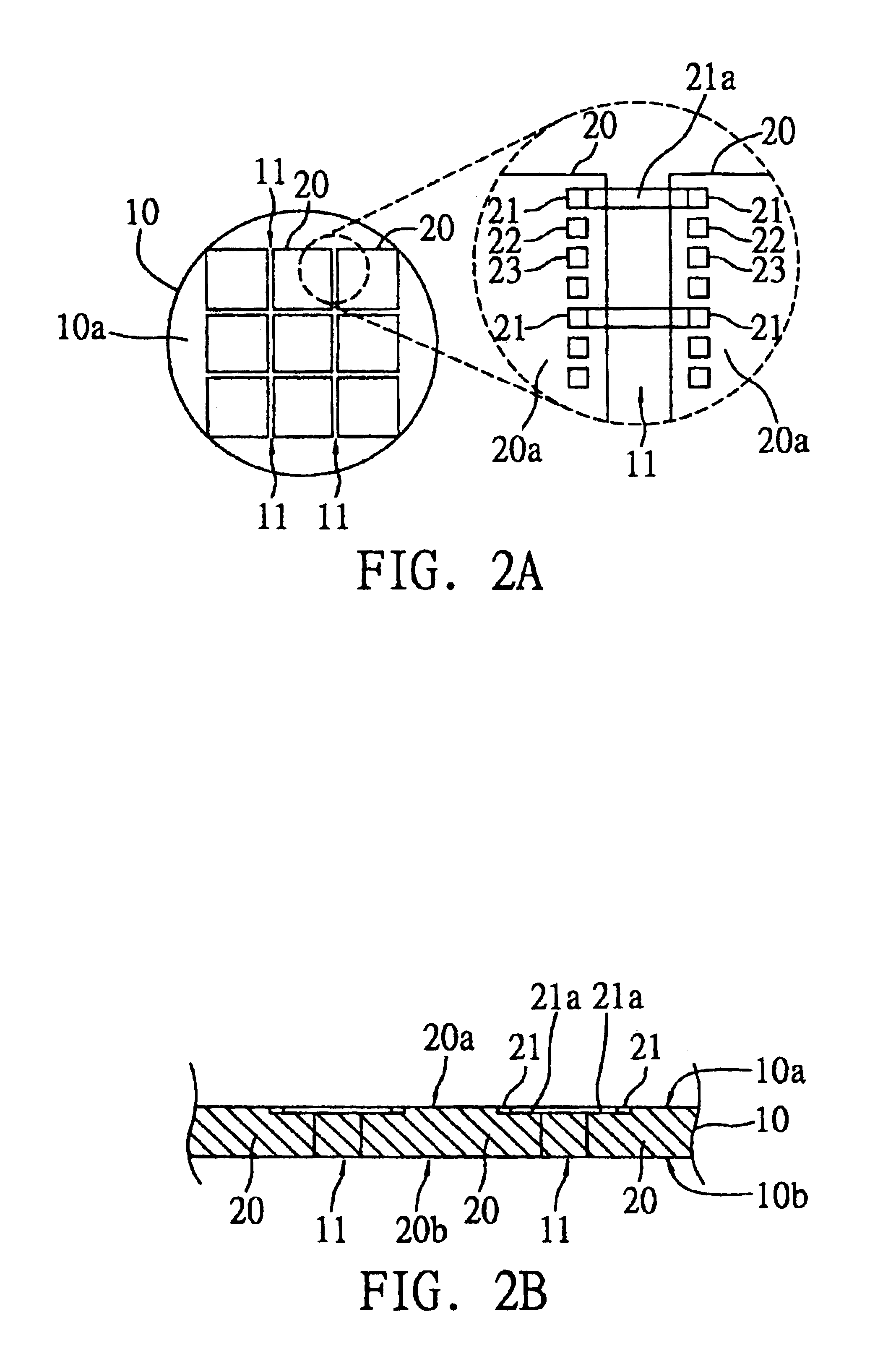
[0024]Referring to FIG. 1, at least one semiconductor chip 20 is mounted on a substrate 50 having a front surface 50a and a back surface 50b, wherein the front surface 50a is formed with at least one grounding plane 51, while the back surface 50b is provided with a plurality of ground-ball pads 52. In addition, the substrate 50 is formed with a plurality of conductive vias 53 for electrically connecting the grounding plane 51 to the ground-ball pads 52. Further, the chip 20 has an active surface 20a and an inactive surface 20b, wherein the active surface 20a is formed with a plurality of ground pads 21 which electrically connect via the conductive traces 21a to the edge of the chip 20 and then electrically connect the electrically-conductive wall 31. The inactive surface 20b of the chip 20 is adhered by mea...


PUM


Abstract

A semiconductor package and a fabrication method thereof are provided, in which a ground pad on a chip is electrically connected to a ground plane on a substrate by means of an electrically-conductive wall formed over a side surface of the chip and an electrically-conductive adhesive used for attaching the chip to the substrate. Therefore, a wire-bonding process is merely implemented for power pads and signal I / O (input / output) pads on the chip without having to form ground wires on the ground pads for electrical connection purposes. This benefit allows the use of a reduced number of bonding wires and simplifies wire arrangement or routability. And, a grounding path from the chip through the electrically-conductive wall and electrically-conductive adhesive to the substrate is shorter than the conventional one of using ground wires, thereby reducing a ground-bouncing effect and improving electrical performances of the semiconductor package.

Description

BACKGROUND OF THE INVENTION[0001]1. Field of the Invention:[0002]This invention relates to semiconductor packaging technology, and more particularly, to a semiconductor package with enhanced chip groundability and method of fabricating the same.[0003]2. Description of Related Art:[0004]Wire-bonding (WB) technology is a widely-used electrical connecting method in chip-packaging processes, which is used to electrically connect an array of pads on the chip, including ground pads, power pads, and signal I / O pads by means of bonding wires to corresponding connecting points on a substrate, so as to allow the internal circuitry of the packaged chip to be electrically connected to external printed circuit board.[0005]One drawback to the conventional electrical connection between a chip and a substrate via bonding wires, however, is that wire routablity would be a problem, particularly in the case of the chip having a great number of densely-arranged ground / power and I / O pads to be electrica...

Claims


Application Information

Patent Timeline
IPC IPC(8): H01L23/50H01L23/48H01L21/60
CPCH01L23/481H01L23/50H01L24/27H01L24/82H01L24/83H01L24/32H01L2924/0665H01L2924/014H01L2924/01033H01L2224/2919H01L2224/2518H01L2224/32225H01L2224/8319H01L2224/838H01L2924/01047H01L2924/01079H01L2924/0781H01L2924/10157H01L2924/14H01L2924/15311H01L2924/00H01L2924/181H01L2924/00012
Inventor WANG, CHIN FATSAI, WEN-TAJOE, YUAN-PING
Owner SILICONWARE PRECISION IND CO LTD
Why Eureka
Try Eureka