Low temperature nitride used as Cu barrier layer

a technology of low temperature nitride and barrier layer, which is applied in the direction of chemical vapor deposition coating, semiconductor/solid-state device details, coatings, etc., can solve the problems of undesired silicide formation in copper, unfavorable increase of copper line resistance, etc., to avoid undesired increase in copper line resistance, increase metal resistance, and enhance chemical vapor deposition

Inactive Publication Date: 2007-03-06
MICRON TECH INC
View PDF9 Cites 5 Cited by
  • Summary
  • Abstract
  • Description
  • Claims
  • Application Information

AI Technical Summary

Benefits of technology

[0016]From the foregoing, it will be appreciated that the aspects of the present invention provide a method of depositing a non-conductive barrier layer onto a metal surface without increasing the resistance of the metal. In particular, the method provides a novel low temperature plasma enhanced chemical vapor deposition (PECVD) process wherein the low temperature processing environment is shown to inhibit the formation of silicide in the copper, thereby avoiding the undesired increase in copper line resistance that will otherwise result from using known PECVD process parameters. These and other objects and advantages of the present invention will become more apparent from the following description taken in conjunction with the following drawings.

Problems solved by technology

Such reaction between the silicon nitride and copper is generally not favored as it results in the formation of silicide in the copper, which in turn will unfavorably increase the line resistance of the copper.
Furthermore, the undesired silicide formation in copper is also known to occur in a reaction between the silane gas used as part of the PECVD process and the exposed copper surface when the PECVD process is conducted in a high temperature environment as taught by prior art.

Method used


Image

  • Low temperature nitride used as Cu barrier layer
  • Low temperature nitride used as Cu barrier layer
  • Low temperature nitride used as Cu barrier layer

Examples


Embodiment Construction

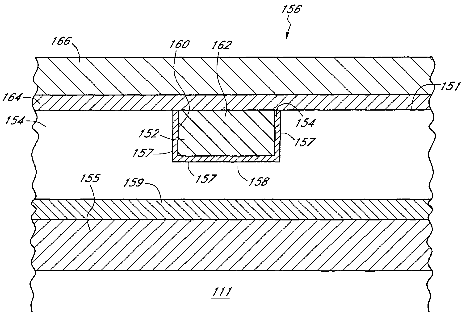
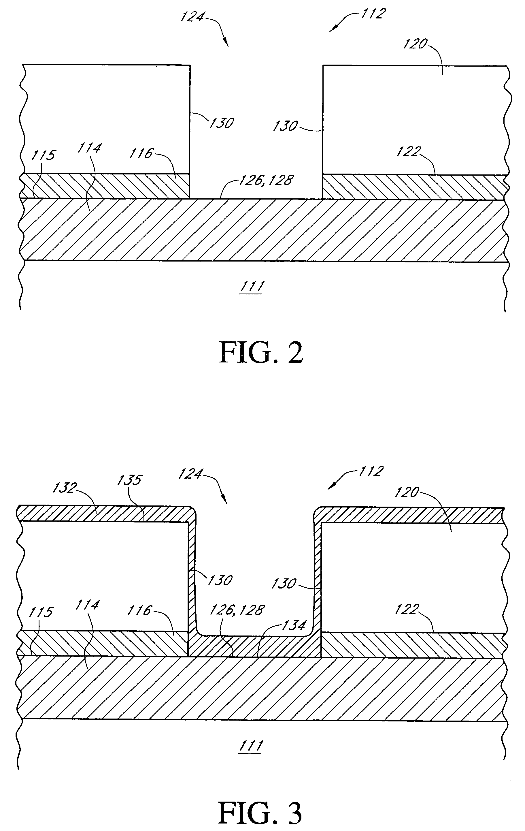
[0026]Reference will now be made to the drawings wherein like numerals refer to like parts throughout. As will be described herein below, the process of the preferred embodiment provides a method of depositing a non-conductive barrier layer onto a copper surface wherein the barrier layer comprises a nitride film.

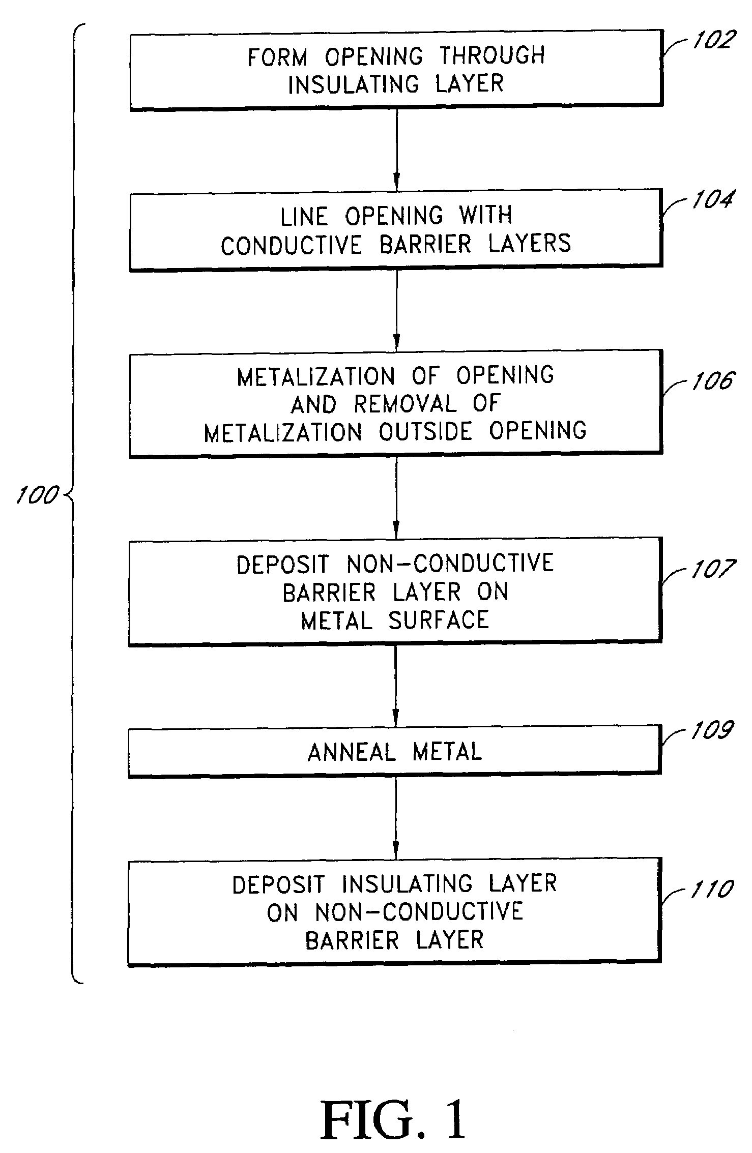
[0027]FIG. 1 schematically illustrates a process flow 100 of the preferred embodiment of forming a non-conductive barrier film between a top surface of a conductive layer and a bottom surface of an insulating layer. As shown in FIG. 1, the process begins with a first step 102 comprising the formation of an opening through an insulating layer. As will be shown in greater detail below, the openings generally extend downwardly from a top surface of the insulating layer so as to either expose an underlying conductive surface for electrical contact or so as to extend into the insulating layer to thereby define a trench adapted to receive a conductive trace. Furthermore, the openi...


PUM

PropertyMeasurementUnit
widthaaaaaaaaaa
aspect ratiosaaaaaaaaaa

Abstract

A method of depositing a non-conductive barrier layer onto a metal surface wherein the resistance of the metal remains substantially unchanged before and after the non-conductive barrier layer deposition. The deposition process provides a low temperature processing environment so as to inhibit the formation of impurities such as silicide in the metal, wherein the silicide can adversely increase the resistance of the underlying metal.

Description

RELATED APPLICATIONS[0001]This application is a divisional of U.S. application Ser. No. 10 / 303,585 filed Nov. 22, 2002, now U.S. Pat. No. 6,984,893 which is a divisional of U.S. application Ser. No. 09 / 503,105, filed Feb. 11, 2000, now U.S. Pat. No. 6,492,267. These prior applications are hereby incorporated by reference in their entireties.BACKGROUND OF THE INVENTION[0002]1. Field of the Invention[0003]This invention relates to integrated circuit processing and, more particularly, to a process for depositing a non-conductive barrier layer such as a nitride film onto a copper surface.[0004]2. Description of the Related Art[0005]A high density integrated circuit typically comprises numerous electrical devices and conductors formed on multiple layers of conducting and semiconducting material that are deposited and patterned in sequence onto a substrate surface. Additionally, insulating material is typically positioned between the individual devices so as to electrically isolated the d...

Claims


Application Information

Patent Timeline
Patent Type & Authority Patents(United States)
IPC IPC(8): H01L21/4763C23C16/34H01L21/318H01L21/768
CPCC23C16/345H01L21/3185H01L23/53295H01L23/53238H01L21/76834H01L2924/0002H01L21/02274H01L21/02211H01L21/02164H01L21/0217H01L21/02167H01L2924/00
Inventor YIN, ZHIPINGZIELINSKI, EDENFISHBURN, FRED
Owner MICRON TECH INC
Why Eureka
Try Eureka