Semiconductor device with shield

a shield and semiconductor technology, applied in the direction of semiconductor devices, semiconductor/solid-state device details, electrical apparatus, etc., can solve the problems of limited miniaturization, thickness of the entire package, miniaturization and the reduction of the thickness and the weight of the package,

Active Publication Date: 2007-03-06
SANYO ELECTRIC CO LTD
View PDF18 Cites 189 Cited by
  • Summary
  • Abstract
  • Description
  • Claims
  • Application Information

AI Technical Summary

Benefits of technology

[0008]In view of the above situation, the present invention provides a solution to the above-mentioned problems, and it is an object of the present invention to provide a technology for addressing the noise problem of the semiconductor device in a simple manner.

Problems solved by technology

However, it is still difficult to achieve the levels of the miniaturization, the reduction of the thickness and the reduction of the weight of the package that are currently desired in the market of the portable electronics products or the like, by employing the conventional CSP.
The existence of the support substrate increases the thickness of the entire package, and thus the miniaturization and the reduction of the thickness and the weight of the package are limited.
Further, this also provides a certain limitation to the improvement on the heat dissipation ability thereof.

Method used


Image

  • Semiconductor device with shield
  • Semiconductor device with shield
  • Semiconductor device with shield

Examples


Embodiment Construction

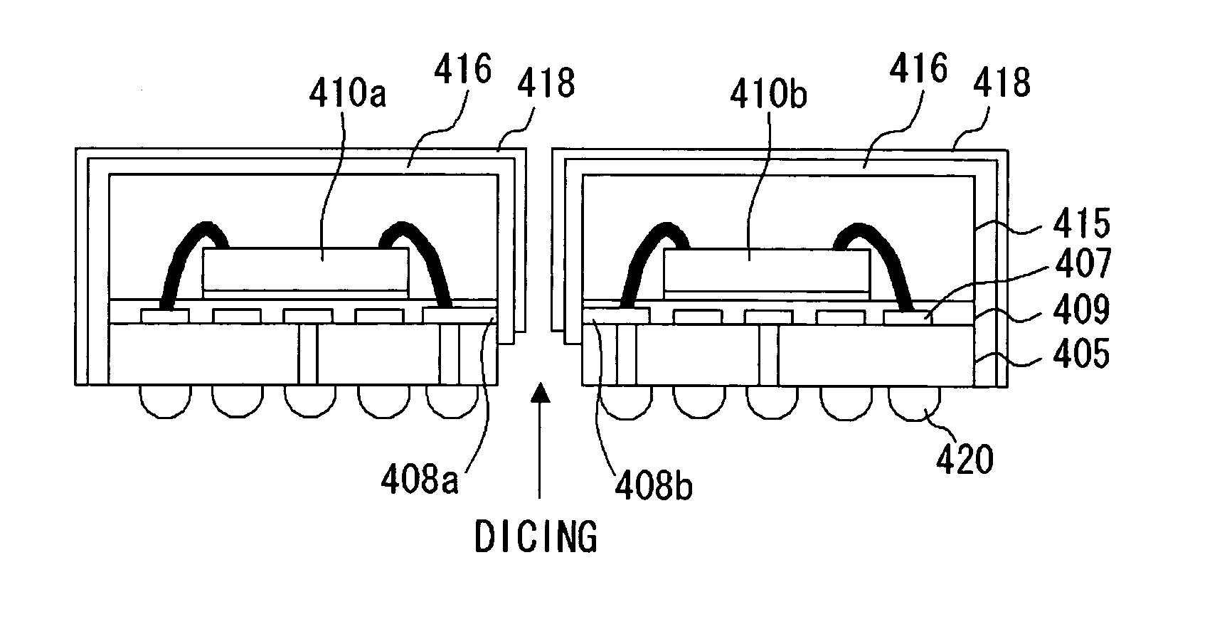
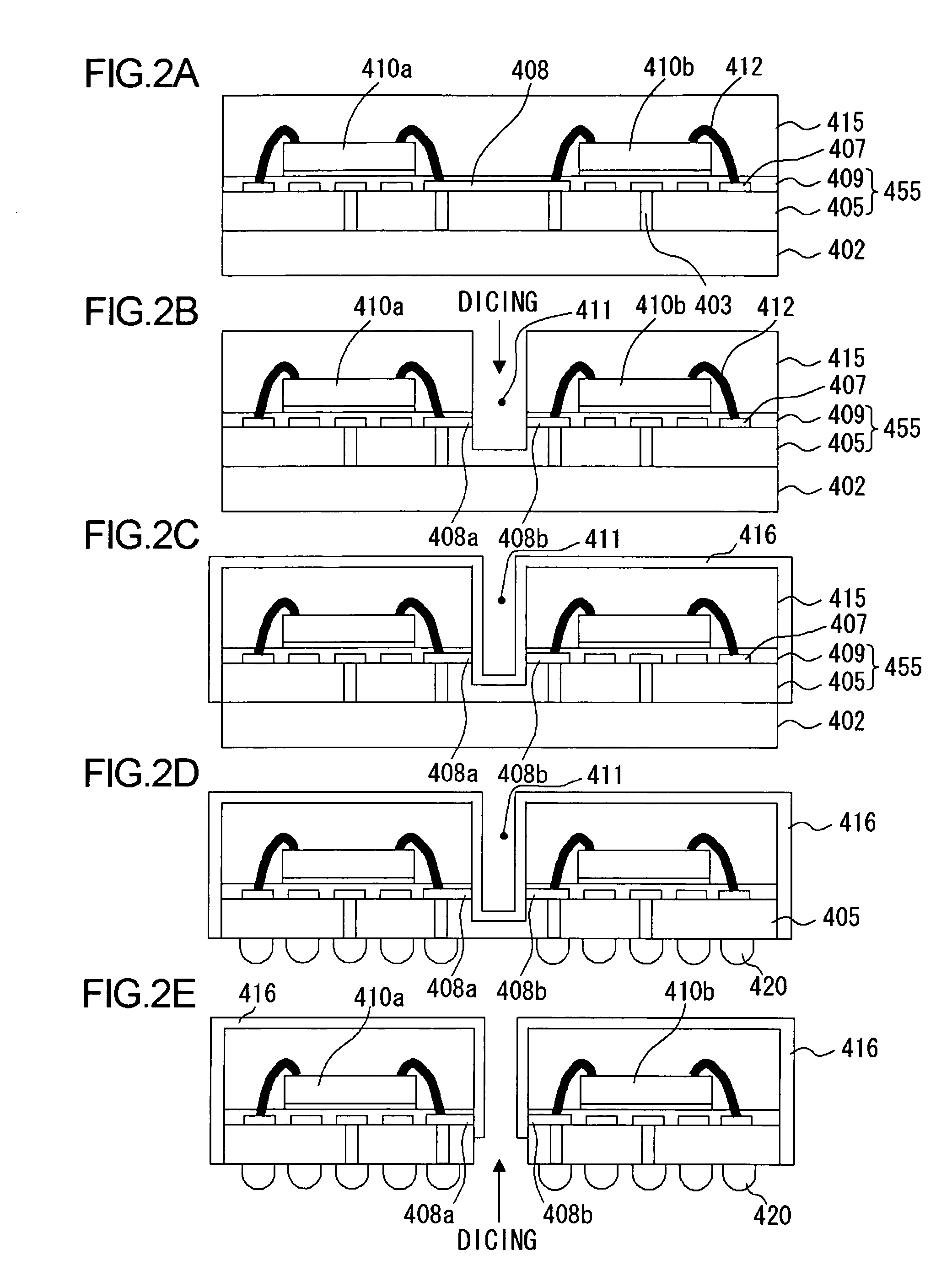
[0042]FIGS. 2A to 2E are cross sectional views of a semiconductor device according to the preferred embodiment of the present invention, showing the process steps for manufacturing the semiconductor device.

[0043]FIG. 2A shows a structure of a multi-layer member in midcourse of the manufacturing of the semiconductor device. Here, the multi-layer member comprises a metal foil 402, a multi-layer interconnect line structure 455 formed thereon, a first circuit element 410a and a second circuit element 410b both formed thereon, and a packaging film 415 formed thereon so as to cover the circuit element 410a and the circuit element 410b. The multi-layer interconnect line structure 455 comprises an interlayer insulating film 405, vias 403 disposed in the interlayer insulating film 405, interconnect lines 407 and an interconnect line 408 both electrically coupled to the vias 403, and an insulating film 409 formed thereon so as to cover the interconnect lines 407 and the interconnect line 408....


PUM


Abstract

The semiconductor device comprises: an interlayer insulating film 405 and an insulating film 409, interconnect lines 407, 408a and 408b embedded in the insulating film 409, circuit elements 410a and 410b mounted on the insulating film 409, a packaging film 415 formed so as to cover the circuit elements 410a and 410b, and an electroconductive shielding film 416 formed so as to cover the packaging film 415. The interconnect lines 408a and 408b are configured to be electrically coupled to the shielding film 416.

Description

[0001]This application is based on Japanese patent application NO.2003-68145, the content of which is incorporated hereinto by reference.BACKGROUND OF THE INVENTION[0002]1. Field of the Invention[0003]The present invention relates to a semiconductor device, which has a circuit element mounted thereon, and a method for manufacturing same.[0004]2. Description of the Related Art[0005]In recent years, portable electronics products such as cellular phone, PDA (personal digital assistant), DVC (digital video camera), DSC (digital still camera) or the like acquire advanced functions in an accelerating speed. Consequently, advanced functions and / or advanced properties are also required for LSI (large-scale integrated circuit) that is employed for these electronics products. Thus, higher frequency for the operating clock of the LSI is correspondingly required. Further, in such condition, the miniaturization and the weight reduction are essential for these products to be accepted by the marke...

Claims


Application Information

Patent Timeline
Patent Type & Authority Patents(United States)
IPC IPC(8): H01L23/552H01L23/31H01L23/498
CPCH01L23/552H01L24/24H01L24/97H01L23/49822H01L23/3128H01L2224/45144H01L2221/68345H01L2224/16H01L2224/24145H01L2224/32225H01L2224/48091H01L2224/48227H01L2224/48463H01L2224/49171H01L2224/73204H01L2224/73265H01L2224/97H01L2924/01005H01L2924/01013H01L2924/0102H01L2924/01029H01L2924/01033H01L2924/01046H01L2924/01047H01L2924/01078H01L2924/01079H01L2924/01082H01L2924/14H01L2924/15311H01L2924/19043H01L2924/19105H01L2924/3025H01L2924/01024H01L2924/01023H01L2924/01006H01L24/49H01L24/48H01L2924/00014H01L2224/85H01L2224/83H01L2924/00H01L2924/00012H01L2924/12042H01L24/45H01L24/73H01L2924/181H01L2224/05554H01L2224/0401
Inventor USUI, RYOSUKE
Owner SANYO ELECTRIC CO LTD
Why Eureka
Try Eureka