Parallel compression test circuit of memory device

a memory device and compression test technology, applied in logic circuits, pulse techniques, instruments, etc., can solve problems such as noise generation and increased peak current, and achieve the effect of reducing nois

Inactive Publication Date: 2007-03-06
SK HYNIX INC
View PDF13 Cites 115 Cited by
  • Summary
  • Abstract
  • Description
  • Claims
  • Application Information

AI Technical Summary

Benefits of technology

[0030]Accordingly, it is an object of the present invention to disperse peak current and reduce noise by operating input / output amplifiers in each bank at different timings.
[0031]It is another object of the present invention to improve reliability of a parallel test mode by operating the same test mode as a normal operation mode.

Problems solved by technology

As a result, since all of the input / output amplifiers 16 are simultaneously operated, the peak current becomes larger and noise is generated.

Method used


Image

  • Parallel compression test circuit of memory device
  • Parallel compression test circuit of memory device
  • Parallel compression test circuit of memory device

Examples


Embodiment Construction

[0043]The present invention will be described in detail with reference to the accompanying drawings.

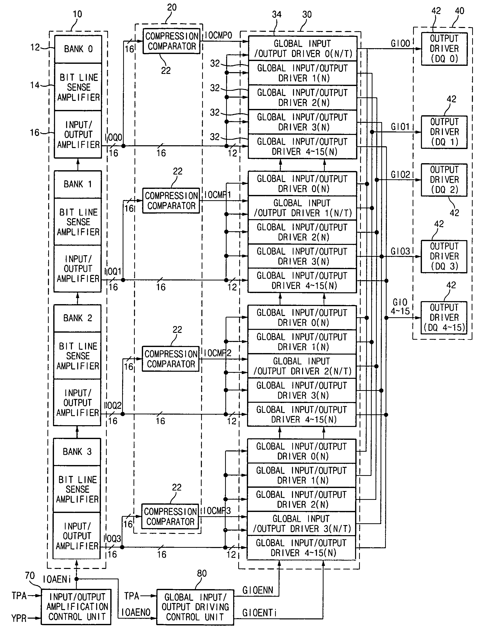
[0044]FIG. 5 is a block diagram illustrating a parallel compression test circuit of a memory device according to an embodiment of the present invention.

[0045]In an embodiment, the parallel compression test circuit of FIG. 5 comprises a memory unit 10, a compression comparing unit 20, a global input / output driving unit 30, an output driving unit 40, an input / output amplification control unit 70 and a global input / output driving control unit 80.

[0046]The memory unit 10 includes four banks 12, bit line sense amplifiers 14 and input / output sense amplifiers 16. Each of the input / output sense amplifiers 16 is activated with a different time difference by an input / output amplification control signal IOAEN outputted from the input / output amplification control unit 70.

[0047]The compression comparing unit 20 compares each data in input / output lines IOQ0˜IOQ3 which is outputted from each bank 12...


PUM


Abstract

A parallel compression test circuit of a memory device disperses peak current and reduce noise by operating input / output amplifiers at different timings in a parallel compression test mode. The parallel compression test circuit comprises an input / output amplification control unit for activating a plurality of input / output amplifiers connected to a selected bank in a normal mode, and activating the plurality of input / output amplifiers in each bank at different timings in a test mode.

Description

BACKGROUND ART[0001]1. Field of the Invention[0002]The present invention generally relates to a parallel compression test circuit of a memory device, and more specifically, to a technology of sequentially operating input / output amplifiers in a parallel compression test to disperse peak current and reduce noise.[0003]2. Description of the Prior Art[0004]FIG. 1 is a block diagram illustrating a conventional parallel compression test circuit of a memory device.[0005]The conventional parallel compression test circuit of FIG. 1 comprises a memory unit 10, a compression comparing unit 20, a global input / output driving unit 30, an output driving unit 40, an input / output amplification control unit 50 and a global input / output driving control unit 60.[0006]The memory unit 10 includes four banks 12, bit line sense amplifiers 14 and input / output sense amplifiers 16. Each of the input / output sense amplifiers 16 is activated by an input / output amplification control signal IOAEN outputted from th...

Claims


Application Information

Patent Timeline
Patent Type & Authority Patents(United States)
IPC IPC(8): H03K19/00
CPCG01R31/31921G11C29/1201G11C29/40G11C29/14G11C2029/2602G01R31/28
Inventor KIM, TAEK SEUNG
Owner SK HYNIX INC
Why Eureka
Try Eureka