
Magnetic annealing of ferromagnetic thin films using induction heating

a technology of ferromagnetic thin films and induction heating, which is applied in the direction of induction heating, furnaces without endless cores, coatings, etc., can solve the problems of complex embedding processes, degrading device performance, and requiring the integration or incorporation of a wide range of possible device structures in the fabrication process

Inactive Publication Date: 2007-03-20
MICHIGAN TECHNOLOGICAL UNIVERSITY
View PDF22 Cites 8 Cited by
  • Summary
  • Abstract
  • Description
  • Claims
  • Application Information

AI Technical Summary

Problems solved by technology

These regions may include ultra-thin ion implanted source and drain regions in a submicron complementary metal-oxide-semiconductor field-effect transistor circuit (CMOS FET), among others, and exposure of such regions to high temperature result in the degradation of device performance.
Thus, material and process related temperature limitations prohibit the integration or incorporation of a wide range of possible device structures in the fabrication process.
Both the drivers and the logic circuits typically have different thermal capacities and, therefore, complicated processes are required to embed the drivers and the logic circuits in a single system.
The incorporation of devices into mainstream processing also presents thermal challenges for integration of the technologies.
However, a microelectronic process typically requires lower temperatures throughout its processing.
The relatively high thermal energy generated in the thermal treatment of the MEMS tends to impact the CMOS processing of the system.
Similarly, embedding elements, like radio-frequency components into high density CMOS, require different thermal treatments and, thus, require complicated processes to embed them together.
Pressure sensors, accelerometers, optoelectronic device assemblies, and some microelectronics technologies require packaging or assemblies that utilize temperatures above 300–400° C., which temperatures could damage microelectronic circuitry.

Method used


Image

  • Magnetic annealing of ferromagnetic thin films using induction heating
  • Magnetic annealing of ferromagnetic thin films using induction heating
  • Magnetic annealing of ferromagnetic thin films using induction heating

Examples


Embodiment Construction

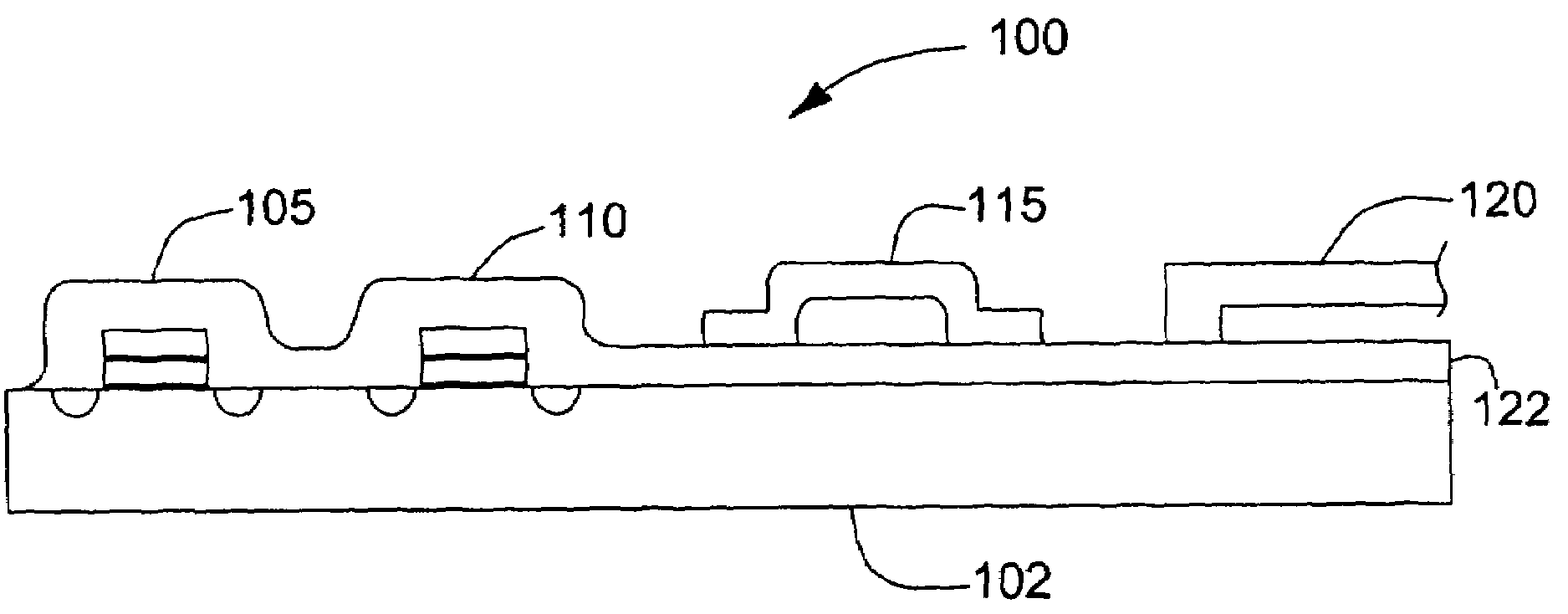
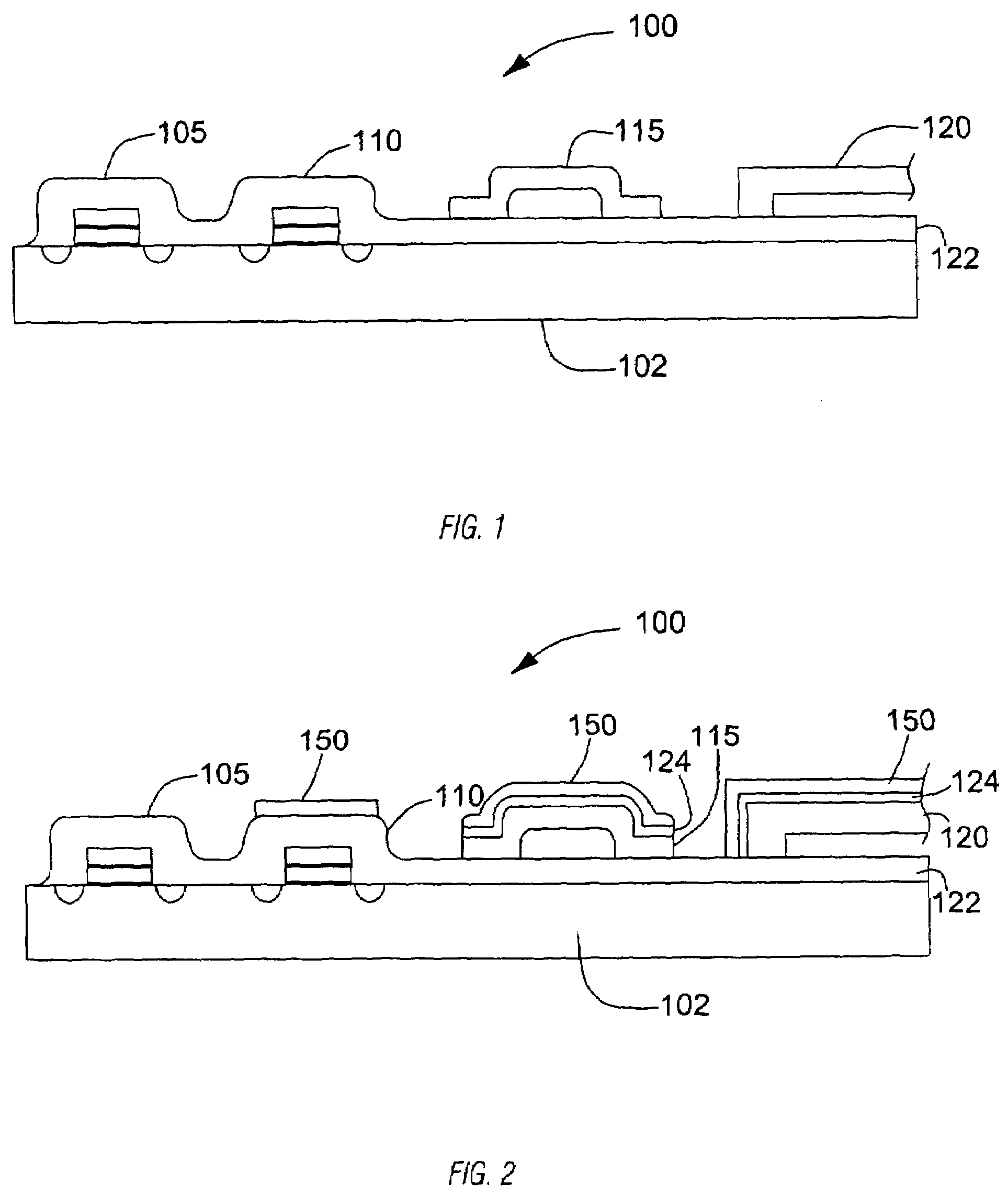
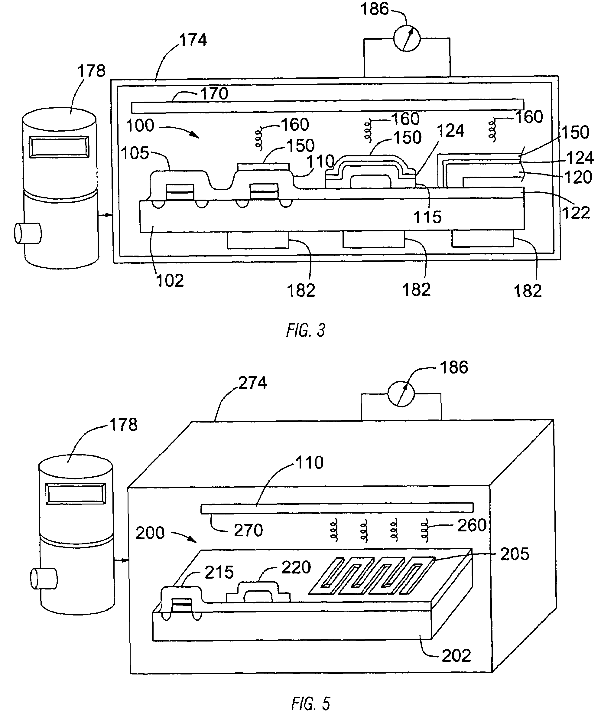
[0018]Before any embodiments of the invention are explained in detail, it is to be understood that the invention is not limited in its application to the details of construction and the arrangement of components set forth in the following description or illustrated in the following drawings. The invention is capable of other embodiments and of being practiced or of being carried out in various ways. Also, it is to be understood that the phraseology and terminology used herein is for the purpose of description and should not be regarded as limiting. The use of “including”, “comprising”, or “having” and variations thereof herein is meant to encompass the items listed thereafter and equivalents thereof as well as additional items. Unless limited otherwise, the terms “connected”, “coupled”, and “mounted” and variations thereof herein are used broadly and encompass direct and indirect connections, couplings, and mountings. In addition, the terms “connected” and “coupled” and variations t...


PUM


Abstract

A method of performing magnetic annealing of a ferromagnetic thin film applied to a substrate includes applying an oscillating magnetic field to the ferromagnetic thin film to induce a current therein and heat the ferromagnetic thin film. A directional magnetic field is applied to the ferromagnetic thin film at the same time as the ferromagnetic thin film is heated, and the ferromagnetic thin film is allowed to acquire a desired magnetic characteristic, and then the oscillating magnetic field is removed and the ferromagnetic thin film is allowed to cool.

Description

CROSS REFERENCE TO RELATED APPLICATIONS[0001]This application claims priority under 35 U.S.C. § 120 to patent application Ser. No. 10 / 376,497, filed on Feb. 28, 2003, which application claims priority under 35 U.S.C. § 119 to provisional patent application No. 60 / 360,667, filed on Mar. 1, 2002. The entire contents of both applications are incorporated herein by reference.BACKGROUND OF THE INVENTION[0002]The present invention relates to induction heating, and magnetic annealing using induction heating.[0003]Ferromagnetic thin films are important components of many microelectronic devices and structures. For example, magnetic random access memories (MRAMs) are magnetic storage devices that store information in the form of magnetization of a ferromagnetic thin film that comprises part of a magneto-resistive sensor. Information can been written into the ferromagnetic thin film and read out by detecting a magneto-resistance of the sensor. MRAMs have been refined to allow increasingly lar...

Claims


Application Information

Patent Timeline
Patent Type & Authority Patents(United States)
IPC IPC(8): H05B6/10H01L21/00H01L21/324H05B6/02
CPCH01L21/324H05B6/105H01L21/67103
Inventor BERGSTROM, PAUL L.TROMBLEY, MELISSA L.
Owner MICHIGAN TECHNOLOGICAL UNIVERSITY
Learn More