Wireless device with distributed load

a wireless device and load technology, applied in the direction of substantially flat resonant elements, high frequency circuit adaptations, resonant antennas, etc., can solve the problems of reducing the efficiency of wireless devices at low frequency ranges, shortening the electrical length of circuit boards in wireless devices, and reducing efficiency

Active Publication Date: 2007-04-03
GOOGLE TECH HLDG LLC
View PDF8 Cites 45 Cited by
  • Summary
  • Abstract
  • Description
  • Claims
  • Application Information

AI Technical Summary

Problems solved by technology

However, shortening the mechanical length of the wireless device results in shortened electrical lengths of circuit boards in the wireless devices.
The shortened electrical length reduces the efficiency of the wireless device at low frequency ranges.
The reduced efficiency results from the lower impedance value of the shortened electrical length, thereby leading to an ineffective resonance setting at lower frequencies.
The problem of reduced efficiency is prevalent in wireless devices having multiple circuit boards, such as “clamshell” devices.

Method used


Image

  • Wireless device with distributed load
  • Wireless device with distributed load
  • Wireless device with distributed load

Examples


first embodiment

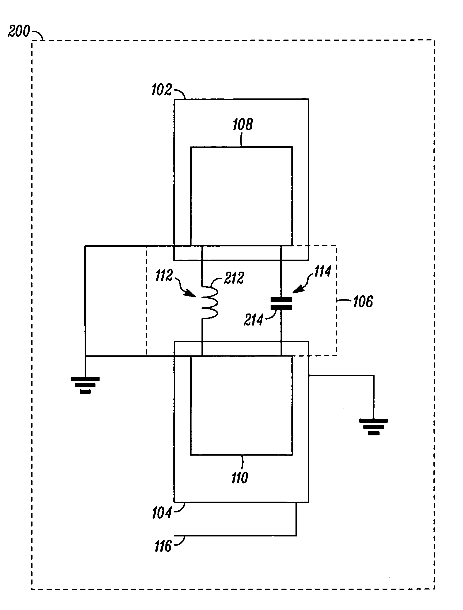
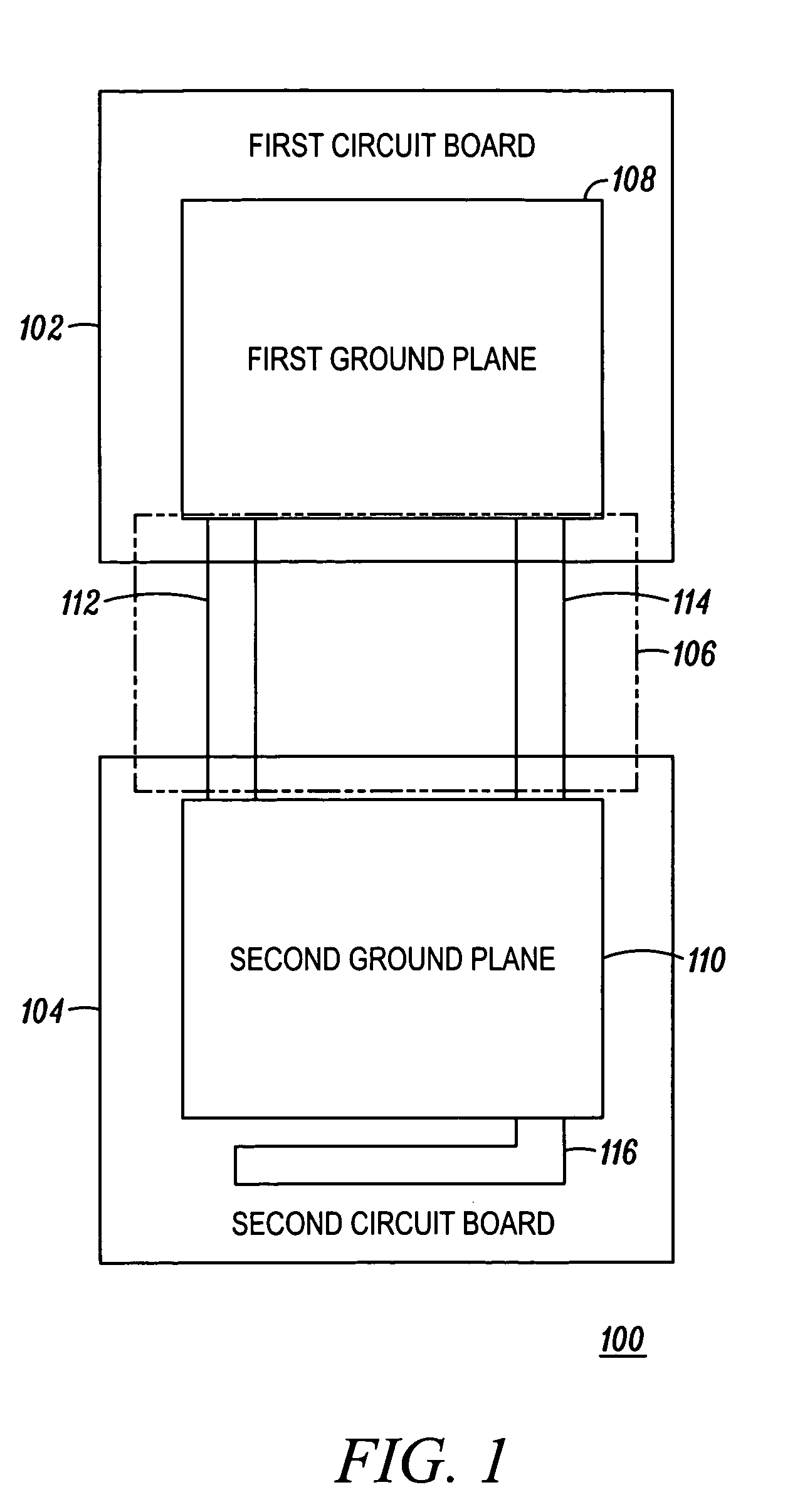
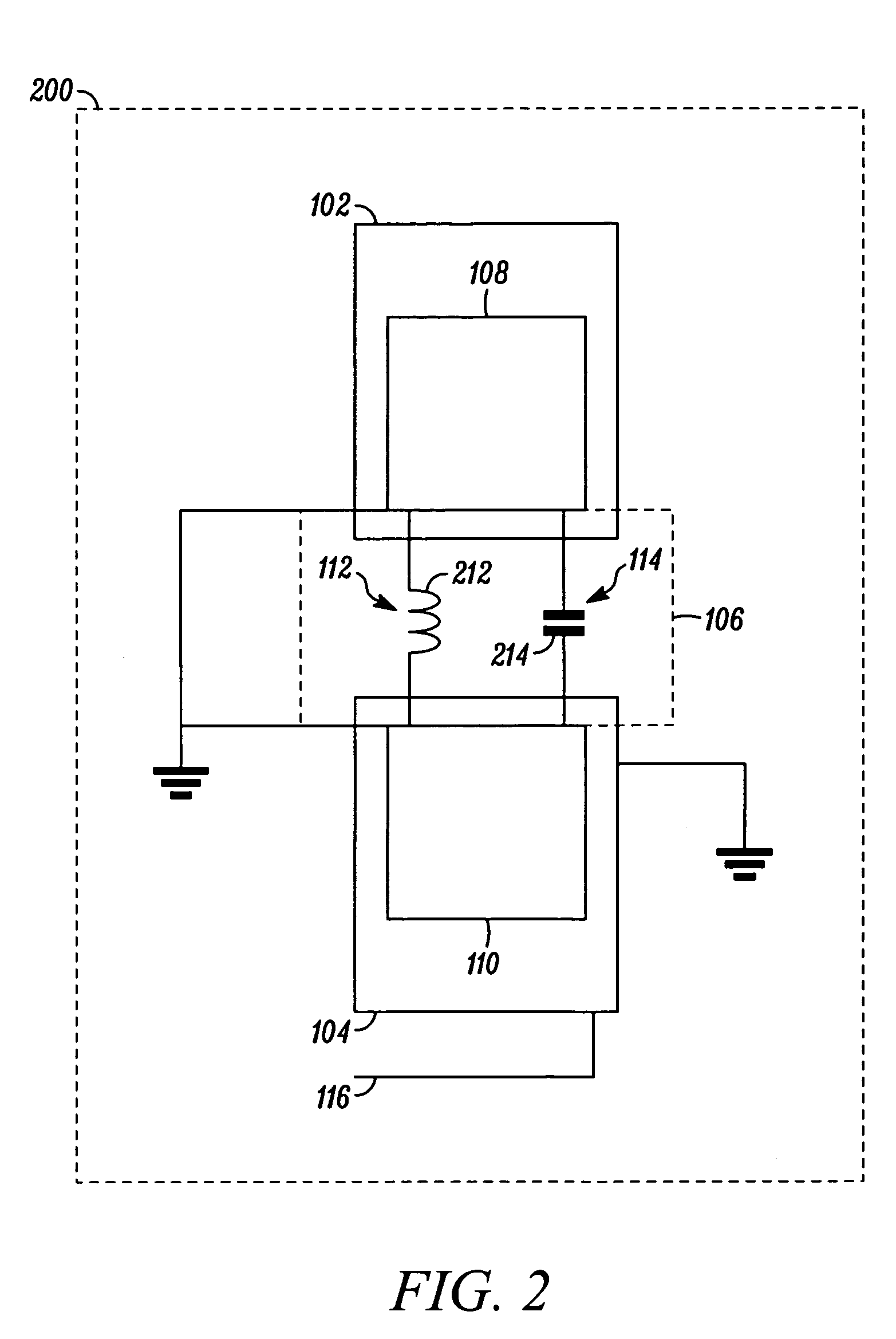
[0021]FIG. 3 shows a block diagram illustrating an exemplary wireless device 300 with a distributed load in accordance with a The wireless device 300 includes a first circuit board 302, a second circuit board 304, and a distributed load 306. The first circuit board 302 includes a first ground plane 308, and the second circuit board 304 includes a second ground plane 310 and an antenna 316. The distributed load 306 has an inductive coupling 312 and a capacitive coupling 314. The capacitive coupling 314 is placed between the first ground plane 308 and the second ground plane 310. The capacitive coupling 314 is physically grounded on the second ground plane 310 but is floating over the first ground plane 308. In this embodiment, a flat patch 318 is used to create a floating connection 320 to form the capacitive coupling 314. In accordance with an embodiment, the flat patch 318 is physically and electrically coupled to the second ground plane 310 and capacitively coupled to the first g...

second embodiment

[0024]FIG. 6 shows a diagram illustrating a capacitive coupling through a cylindrical capacitive coupler in accordance with the second detailed embodiment as shown in FIG. 5. In this second embodiment, the capacitive coupling 514 shown in FIG. 5 is implemented as an air gap 614 between a metal finger 615 physically and electrically coupled to the first circuit board 502 and a conductive barrel 620 physically and electrically coupled to the second circuit board 504. The first circuit board 502 and the second circuit board 504 are connected using a pair of hinges: a first hinge 602 and a second hinge 604. In this embodiment, the pair of hinges is placed opposite to where the antenna 516 (not shown in FIG. 6) is placed in the second circuit board 504. The first hinge 602 supports the inductive coupling 512 (not shown in FIG. 6), and the second hinge 604 supports the capacitive coupling 514. The distributed load 506, as supported by the pair of hinges, 602, 604 produces sufficient imped...


PUM


Abstract

A wireless device (100) includes a first circuit board (102), a second circuit board (104), and a distributed load (106) having an inductive coupling (112) and a capacitive coupling (114). The inductive coupling (112) and the capacitive coupling (114) form a parallel resonance at predefined frequencies of interest. The second circuit board (104) includes an antenna (116) for receiving and transmitting radio waves.

Description

FIELD OF THE INVENTION[0001]The present invention generally relates to wireless devices and more specifically, to an apparatus for tuning impedance in wireless devices.BACKGROUND OF THE INVENTION[0002]An antenna plays an important role in providing reliable communication in a wireless device. The growing trend of incorporating antennae in the bodies of wireless devices has increased the size of the wireless devices. This trend goes against the modern norms of having smaller-sized wireless devices with increased aesthetic value. One way to increase the aesthetic value of the wireless device is to shorten the mechanical length of the wireless device. However, shortening the mechanical length of the wireless device results in shortened electrical lengths of circuit boards in the wireless devices. The shortened electrical length reduces the efficiency of the wireless device at low frequency ranges. The reduced efficiency results from the lower impedance value of the shortened electrical...

Claims


Application Information

Patent Timeline
Patent Type & Authority Patents(United States)
IPC IPC(8): H01Q1/24
CPCH01Q1/243H01Q9/42H05K1/14H04M1/0214H05K2201/09318H05K1/0239H05K1/148H05K1/0237H01Q9/0407
Inventor LIU, HONGWEINAPOLES, ADRIANWHITE, BENJAMIN O.
Owner GOOGLE TECH HLDG LLC
Why Eureka
Try Eureka