Random access memory device utilizing a vertically oriented select transistor

a random access memory and select transistor technology, applied in semiconductor devices, digital storage, instruments, etc., can solve the problem of limited memory density, achieve the effect of preventing the loss of storage cell data, preserving array efficiency, and preventing leakag

Inactive Publication Date: 2007-04-17
OVONYX MEMORY TECH LLC
View PDF14 Cites 61 Cited by
  • Summary
  • Abstract
  • Description
  • Claims
  • Application Information

AI Technical Summary

Benefits of technology

[0012]The present invention provides higher density memory arrays using vertical technology in fabricating the access transistors to provide memory bits with minimal leakage, thereby preventing the loss of storage cell data while preserving array efficiency. Further, alpha-particle induced soft errors that alter the data stored in the memory cells are reduced and simplified fabrication techniques also are provided.

Problems solved by technology

The lack of an access transistor, however, exposes MRAM cells to “sneak” currents through unselected cells, which requires compensation by sense circuitry in order to isolate the selected MRAM cell.
Memory density typically is limited by current processing technologies used for fabricating the memory arrays.

Method used


Image

  • Random access memory device utilizing a vertically oriented select transistor
  • Random access memory device utilizing a vertically oriented select transistor
  • Random access memory device utilizing a vertically oriented select transistor

Examples


Embodiment Construction

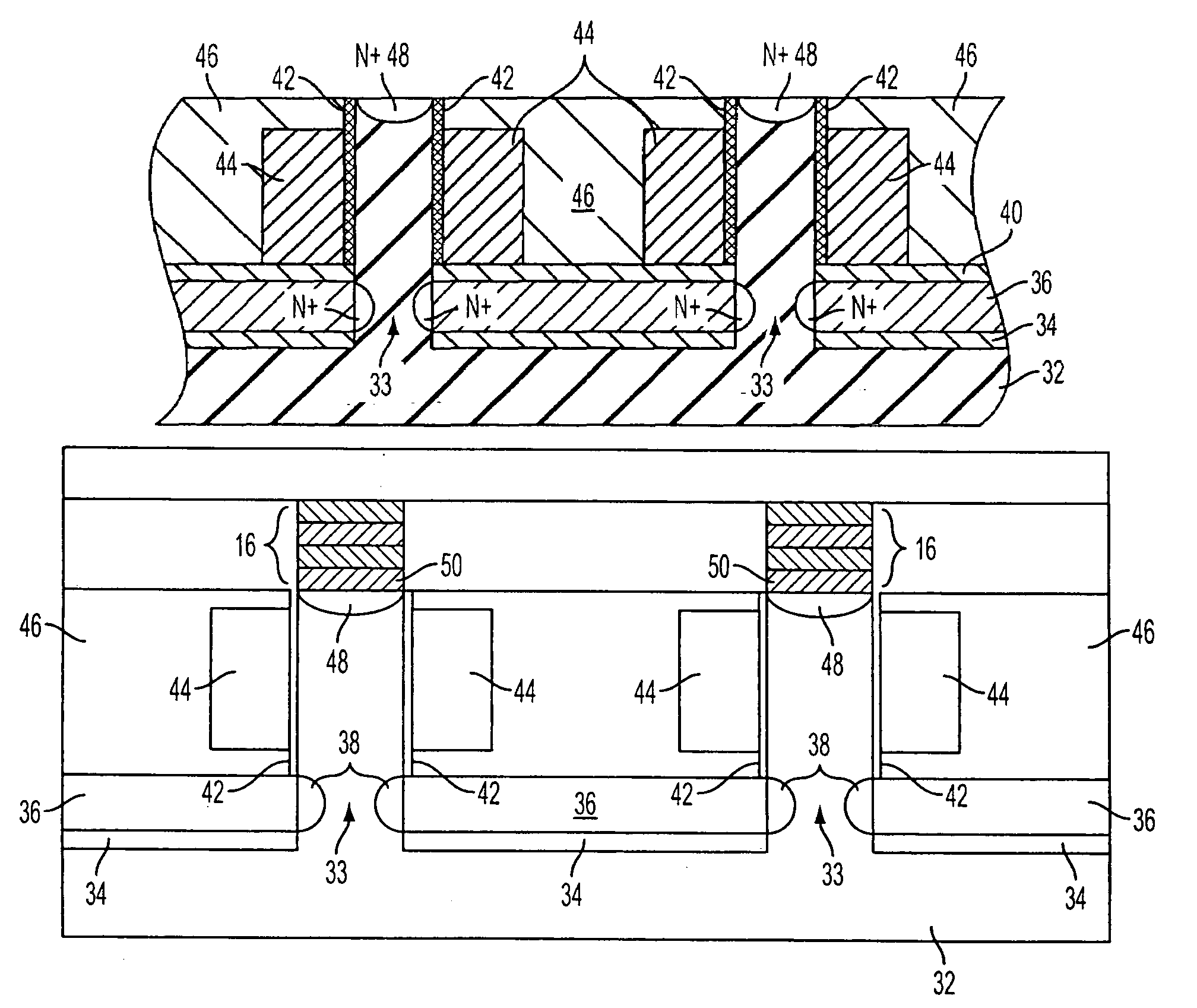
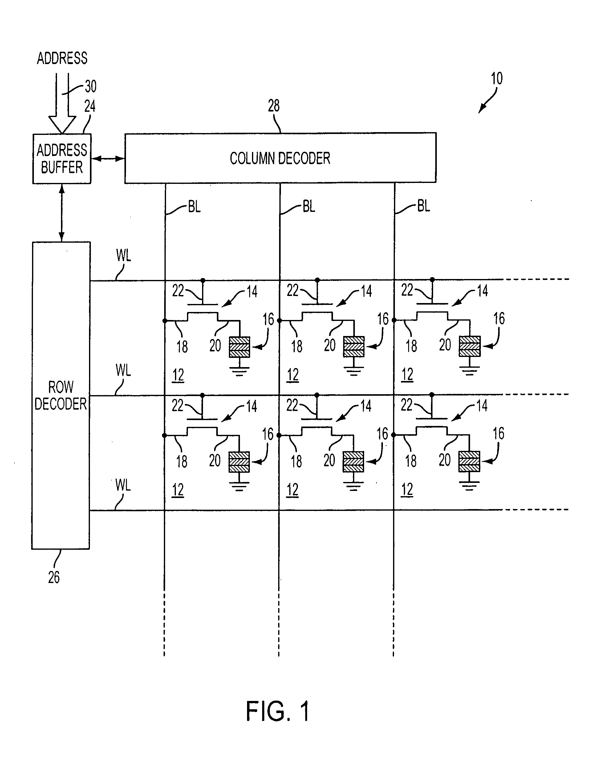
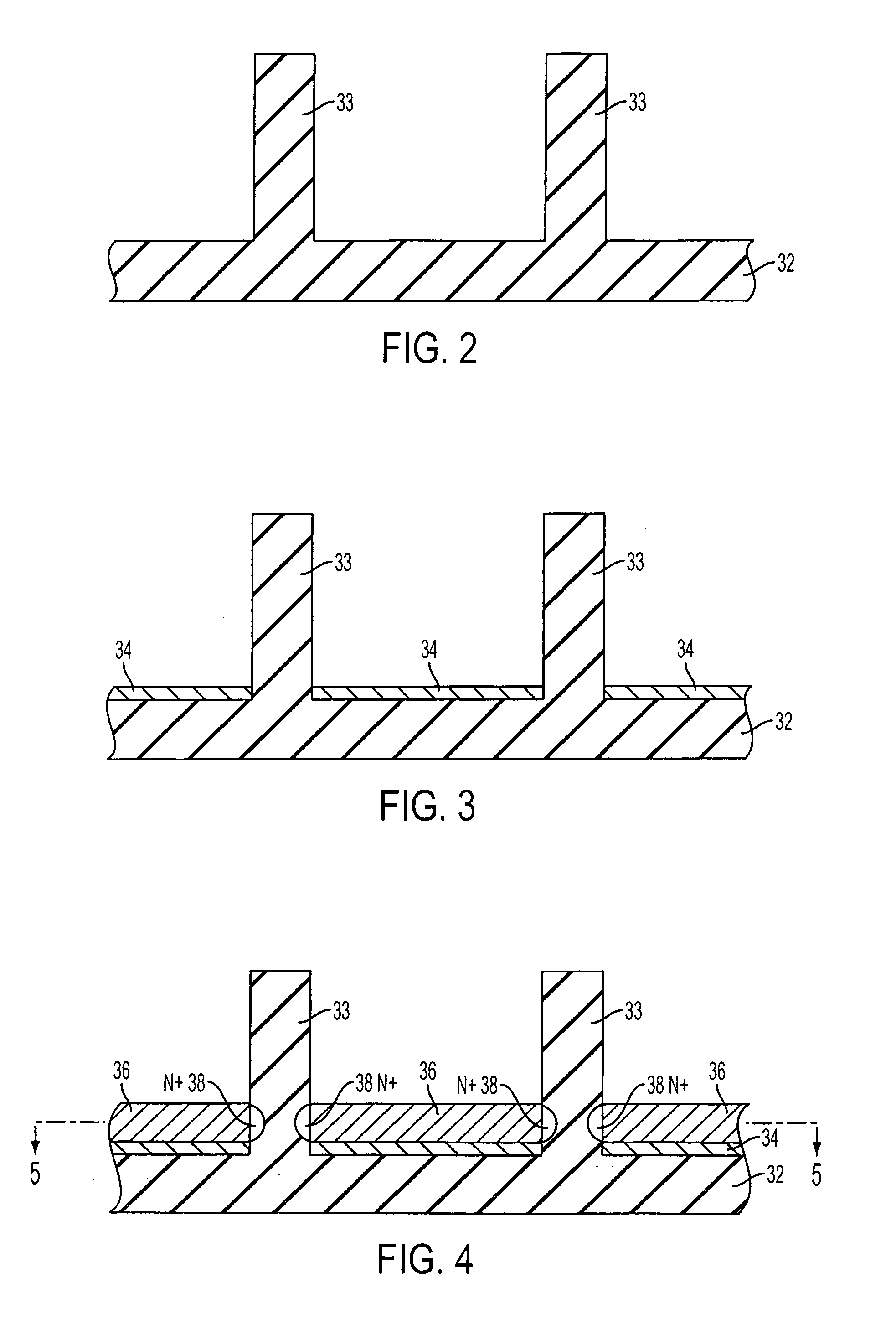
[0022]One or more specific embodiments of the present invention will be described below. In an effort to provide a concise description of these embodiments, not all features of an actual implementation are described in the specification. It should be appreciated that in the development of any such actual implementation, as in any engineering or design project, numerous implementation-specific decisions must be made to achieve the developers' specific goals, such as compliance with system-related and business-related constraints, which may vary from one implementation to another. Moreover, it should be appreciated that such a development effort might be complex and time consuming, but would nevertheless be a routine undertaking of design, fabrication, and manufacture for those of ordinary skill having the benefit of this disclosure.

[0023]The terms “wafer” and “substrate” are to be understood as interchangeable and as including silicon, silicon-on-insulator (SOI) or silicon-on-sapphir...


PUM


Abstract

A memory structure has a vertically oriented access transistor with an annular gate region. A transistor is fabricated such that the channel of the transistor extends outward with respect to the surface of the substrate. An annular gate is fabricated around the vertical channel such that it partially or completely surrounds the channel. A buried annular bitline may also be implemented. After the vertically oriented transistor is fabricated with the annular gate, a storage device may be fabricated over the transistor to provide a memory cell.

Description

RELATED APPLICATIONS[0001]This application is a continuation-in-part of U.S. patent application Ser. No. 10 / 230,568 filed Aug. 29, 2002 now U.S. Pat. No. 6,794,699, the disclosure of which is incorporated herein by reference.BACKGROUND OF THE INVENTION[0002]1. Field of the Invention[0003]The present invention relates to memory devices, and more specifically, to random access memory devices having vertical access transistors.[0004]2. Description of the Related Art[0005]Semiconductor memory devices are widely used for storing data in systems such as computer systems. Random access memory devices include dynamic random access memory (DRAM), magnetic random access memory (MRAM) and programmable conductor random access memory (PCRAM) memory cells that are being developed for non-volatile data storage in computers and other information processing devices.[0006]A DRAM cell typically includes an access device, such as a field effect transistor (FET), which is coupled to a storage device, su...

Claims


Application Information

Patent Timeline
Patent Type & Authority Patents(United States)
IPC IPC(8): H01L27/108G11C11/24G11C11/404H01L21/336H01L21/8242H01L27/02H01L29/423H01L29/76H01L29/78
CPCG11C11/404H01L27/10823H01L27/10876H01L27/10885H01L29/4238H01L29/66666H01L29/7827H01L27/0207H01L27/10814H01L27/10852H10B63/34H10B61/22H10B12/34H10B12/315H10B12/053H10B12/033H10B12/482
Inventor VOSHELL, THOMAS W.BISSEY, LUCIEN J.DUESMAN, KEVIN G.
Owner OVONYX MEMORY TECH LLC
Why Eureka
Try Eureka