Structure and method for fabricating GaN devices utilizing the formation of a compliant substrate

a technology of compliant substrates and gan devices, which is applied in the direction of semiconductor devices, semiconductor/solid-state device details, electrical equipment, etc., can solve the problems of low crystalline quality of monocrystalline materials, lack of bulk substrates formed of suitable lattice-matched materials for subsequent high-quality epitaxial gan growth, and small size of sic substrates

Inactive Publication Date: 2007-05-01
NXP USA INC
View PDF747 Cites 14 Cited by
  • Summary
  • Abstract
  • Description
  • Claims
  • Application Information

AI Technical Summary

Problems solved by technology

These attempts have generally been unsuccessful because lattice mismatches between the host crystal and the grown crystal have caused the resulting layer of monocrystalline material to be of low crystalline quality.
One significant challenge to large scale production of cubic GaN devices is the lack of bulk substrates formed of suitable lattice-matched material for subsequent high quality epitaxial GaN growth.
SiC substrates are of small size and are expensive.
These significant differences lead to mechanical stresses in the subsequent film growth above the critical thickness, which results in fracturing and voids in the GaN layer.
Another disadvantage of typical GaN films grown on sapphire is the high number of defect dislocations in the GaN layers.
These defects impact the electrical and optical performance of the GaN devices.
In electrical devices, dislocations can create deep defect energy levels that increase the leakage current.

Method used


Image

  • Structure and method for fabricating GaN devices utilizing the formation of a compliant substrate
  • Structure and method for fabricating GaN devices utilizing the formation of a compliant substrate
  • Structure and method for fabricating GaN devices utilizing the formation of a compliant substrate

Examples


example 2

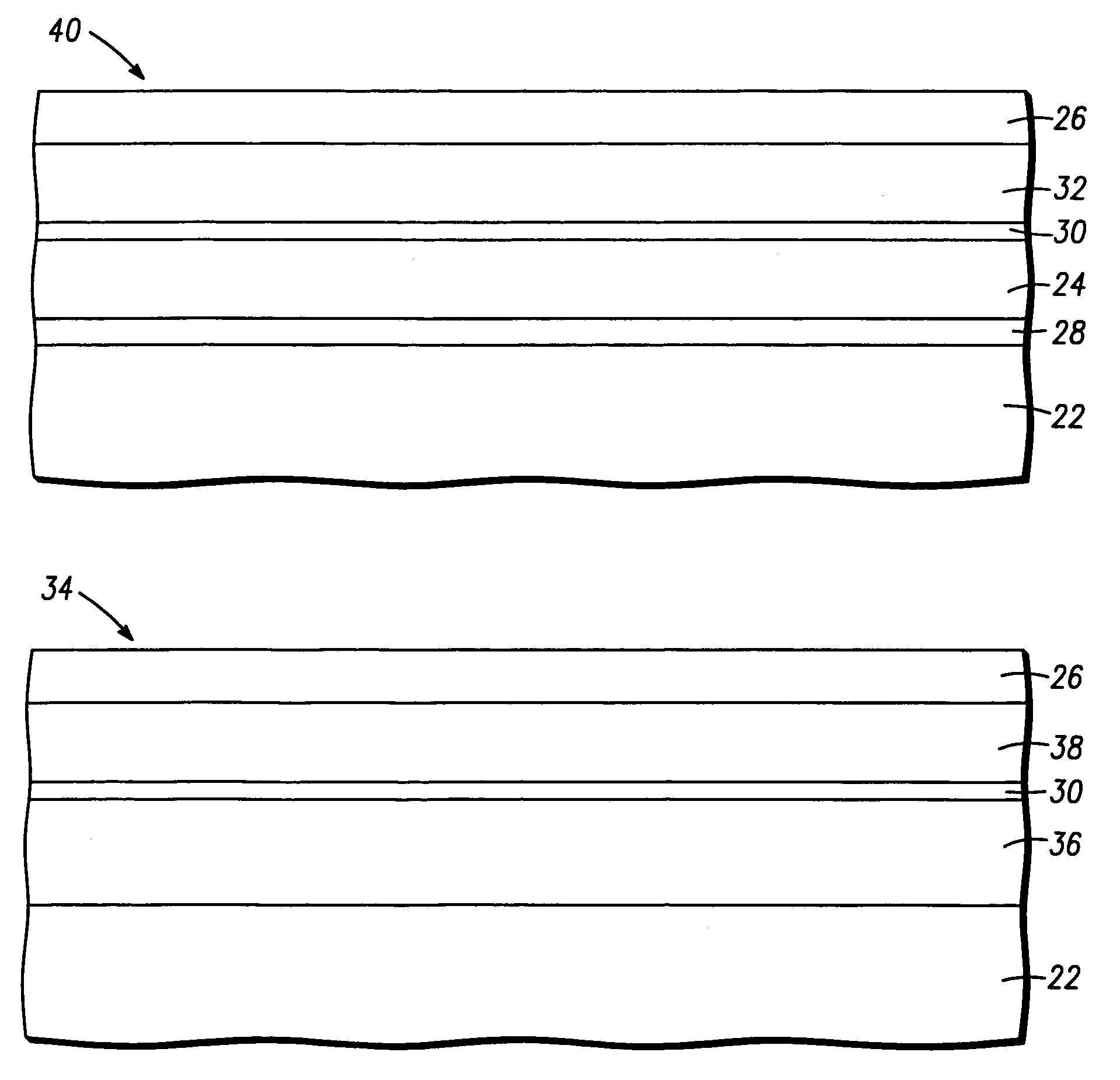
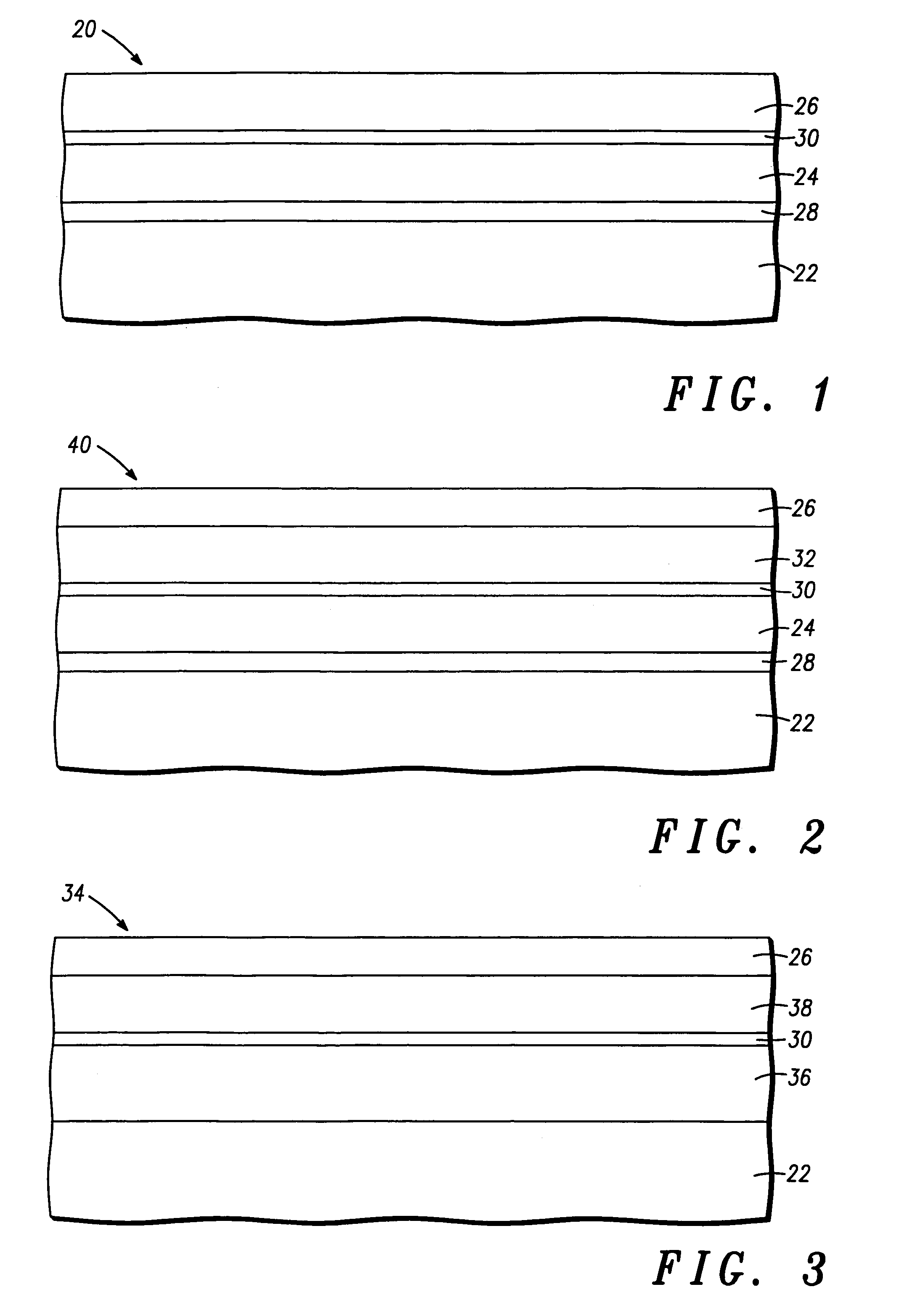
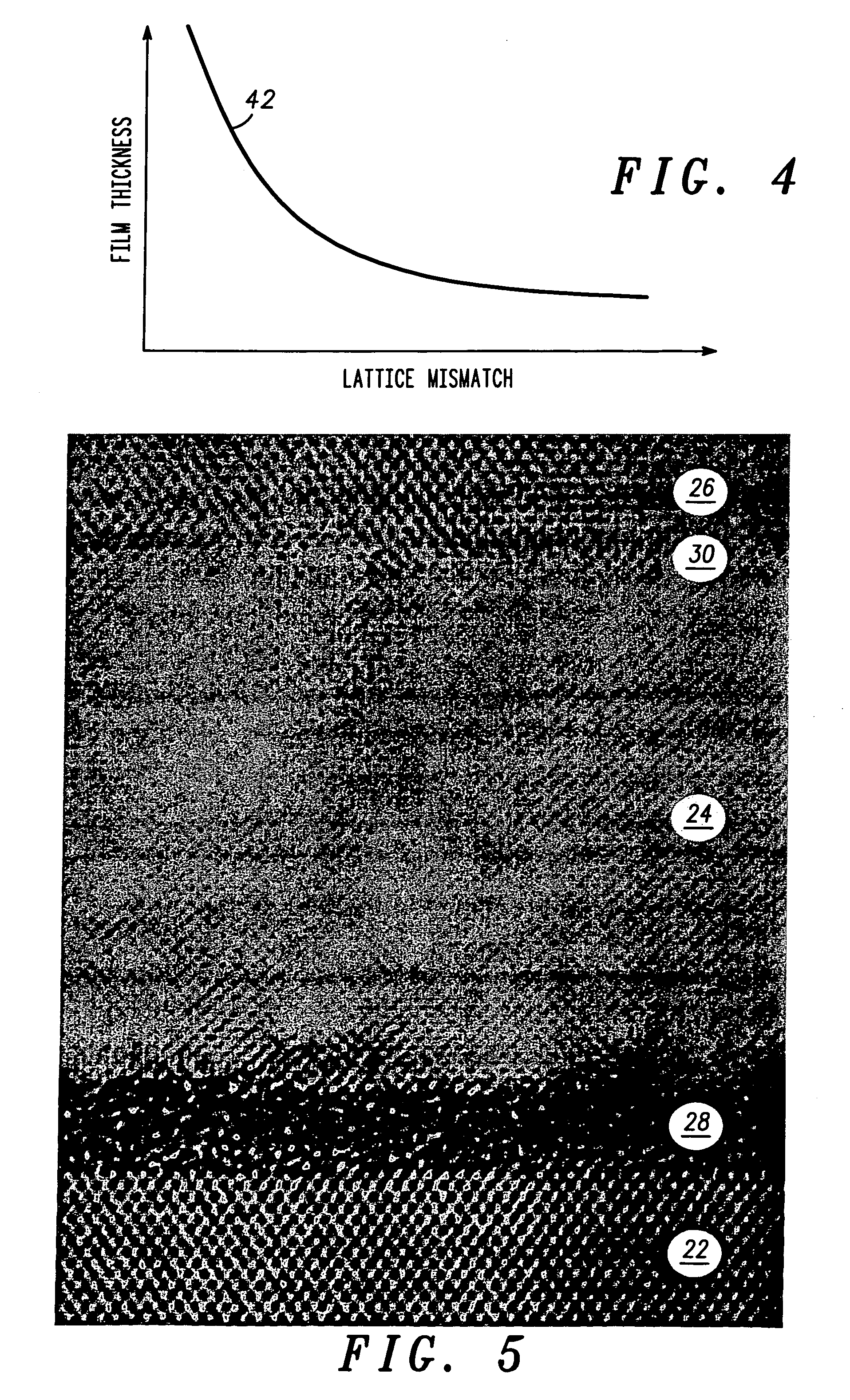
[0040]This embodiment of the invention is an example of structure 40 illustrated in FIG. 2. Substrate 22, accommodating buffer layer 24, and monocrystalline material layer 26 can be similar to those described in example 1. In addition, an additional buffer layer 32 serves to alleviate any strains that might result from a mismatch of the crystal lattice of the accommodating buffer layer and the lattice of the monocrystalline material. Buffer layer 32 can be a layer of germanium or a GaAs, an aluminum gallium arsenide (AlGaAs), an indium gallium phosphide (InGaP), an aluminum gallium phosphide (AlGaP), an indium gallium arsenide (InGaAs), an aluminum indium phosphide (AlInP), a gallium arsenide phosphide (GaAsP), or an indium gallium phosphide (InGaP) strain compensated superlattice. In accordance with one aspect of this embodiment, buffer layer 32 includes a GaAsxP1−x superlattice, wherein the value of x ranges from 0 to 1. In accordance with another aspect, buffer layer 32 includes ...

example 3

[0041]This example provides exemplary materials useful in structure 34, as illustrated in FIG. 3. Substrate material 22, template layer 30, and monocrystalline material layer 26 may be the same as those described above in connection with example 1.

[0042]Amorphous layer 36 is an amorphous oxide layer which is suitably formed of a combination of amorphous intermediate layer materials (e.g., layer 28 materials as described above) and accommodating buffer layer materials (e.g., layer 24 materials as described above). For example, amorphous layer 36 may include a combination of SiOx and SrzBa1−zTiO3 (where z ranges from 0 to 1), which combine or mix, at least partially, during an anneal process to form amorphous oxide layer 36.

[0043]The thickness of amorphous layer 36 may vary from application to application and may depend on such factors as desired insulating properties of layer 36, type of monocrystalline material comprising layer 26, and the like. In accordance with one exemplary aspe...


PUM

PropertyMeasurementUnit
thicknessaaaaaaaaaa
thicknessaaaaaaaaaa
diameteraaaaaaaaaa

Abstract

High quality epitaxial layers of GaN can be grown overlying large silicon wafers (200) by forming an amorphous layer (210) on the substrate. The amorphous layer dissipates strain and permits the growth of a high quality GaN layer (208). Any lattice mismatch between the GaN layer and the underlying substrate is taken care of by the amorphous layer.

Description

[0001]This application is a Continuation of U.S. application Ser. No. 09 / 766,046, filed Jan. 19, 2001 now abandoned, which is a National Stage of PCT / US01 / 46663 filed Dec. 6, 2001.FIELD OF THE INVENTION[0002]This invention relates generally to semiconductor structures and devices and to a method for their fabrication, and more specifically to fabrication of semiconductor structures formed of GaN films on compliant substrates.BACKGROUND OF THE INVENTION[0003]Semiconductor devices typically include multiple layers of conductive, insulating, and semiconductive layers. Often, the desirable properties of such layers improve with the crystallinity of the layer. For example, the electron mobility and optical properties of semiconductive layers improves as the crystallinity of the layer increases. Similarly, the free electron concentration of conductive layers and the electron charge displacement and electron energy recoverability of insulative or dielectric films improves as the crystallin...

Claims


Application Information

Patent Timeline
Patent Type & Authority Patents(United States)
IPC IPC(8): H01L29/76H01L21/20H01L21/316H01L21/318H01L33/00
CPCH01L21/02381H01L21/02458H01L21/02488H01L21/02505H01L21/02513H01L21/02521H01L21/0254H01L21/31691H01L21/3185H01L33/007H01L21/02197H01L21/0217H01L21/02293H01L21/02178H01L21/02356
Inventor RAMDANI, JAMALHILT, LYNDEE L.
Owner NXP USA INC
Why Eureka
Try Eureka