Crystallographic recess etch for embedded semiconductor region

a crystallographic recess and semiconductor technology, applied in the field of semiconductor structures with at least one embedded semiconductor region, can solve the problems of junction leakage current to increase by orders of magnitude, facets on the semiconductor surface, adverse impact on the fet performance,

Inactive Publication Date: 2008-10-02
IBM CORP
View PDF6 Cites 108 Cited by
  • Summary
  • Abstract
  • Description
  • Claims
  • Application Information

AI Technical Summary

Benefits of technology

[0034]A bottom surface of a spacer of an insulated gate field effect transistor (IGFET) may be exposed.

Problems solved by technology

Therefore, the rate of growth in an epitaxy process is often anisotropic, i.e., different along different crystallographic orientations, often causing facets on the semiconductor surface as a result.
The absence of the embedded semiconductor material above the pegging line P has an adverse impact on the FET performance.
Further, junction depth increases by the depth of the pegging line P near the STI after the source and drain ion implantation, which may cause junction leakage current to increases by orders of magnitude.

Method used


Image

  • Crystallographic recess etch for embedded semiconductor region
  • Crystallographic recess etch for embedded semiconductor region
  • Crystallographic recess etch for embedded semiconductor region

Examples


second embodiment

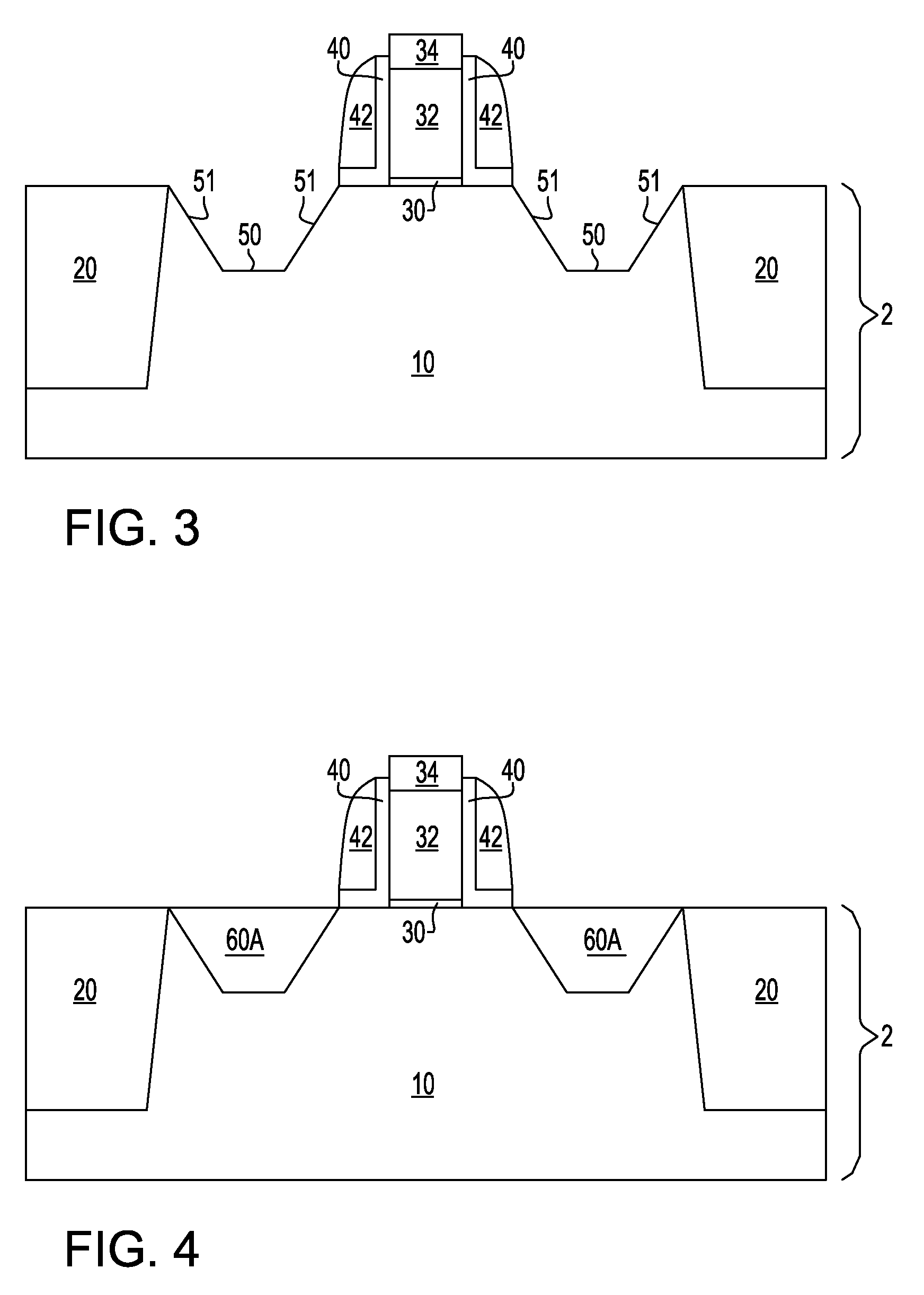
[0063]Referring to FIG. 6, a second exemplary structure according to the present invention is shown. The semiconductor structure in FIG. 6 is formed by extending the crystallographic anisotropic etch after the first exemplary semiconductor structure shown in FIG. 3 is formed. The low etch rate crystallographic facet 51 in FIG. 3 extends further downward until the high etch rate crystallographic facet 50 is reduced to a ridge that joins the two low etch rate crystallographic facets 51. A V-shaped groove with a ridge in the middle is formed by the two low etch rate crystallographic facets 51 in an exposed semiconductor area. Thus, the crystallographic anisotropic etch produces at least one cavity surrounded by crystallographic facets adjoined by a ridge on the substrate semiconductor region 10.

[0064]Referring to FIG. 7, an embedded semiconductor material is deposited on the low etch rate crystallographic facets 51 of the substrate semiconductor region 10 preferably by selective epitax...

first embodiment

[0065]Through the same mechanism as in the first embodiment, the strained embedded semiconductor region 60B exerts stress on neighboring semiconductor structures. Also, the variety of the material that may be used for the embedded triangular semiconductor region 60B is determined by the crystal structure and the lattice constant of the substrate semiconductor region 10.

[0066]As in the first embodiment, each of the facets 51 (in FIG. 6) of the substrate semiconductor region 10 adjoins a facet of the triangular embedded semiconductor region 60B that is located directly across the boundary between the trapezoidal embedded semiconductor region 60B and the substrate semiconductor region 10. At a ridge where two facets belonging to the substrate semiconductor region 10 are adjoined, two other facets belonging to the triangular embedded semiconductor region 60B are also adjoined.

[0067]Referring to FIG. 8, a variant of the second exemplary semiconductor structure is shown, wherein the selec...

third embodiment

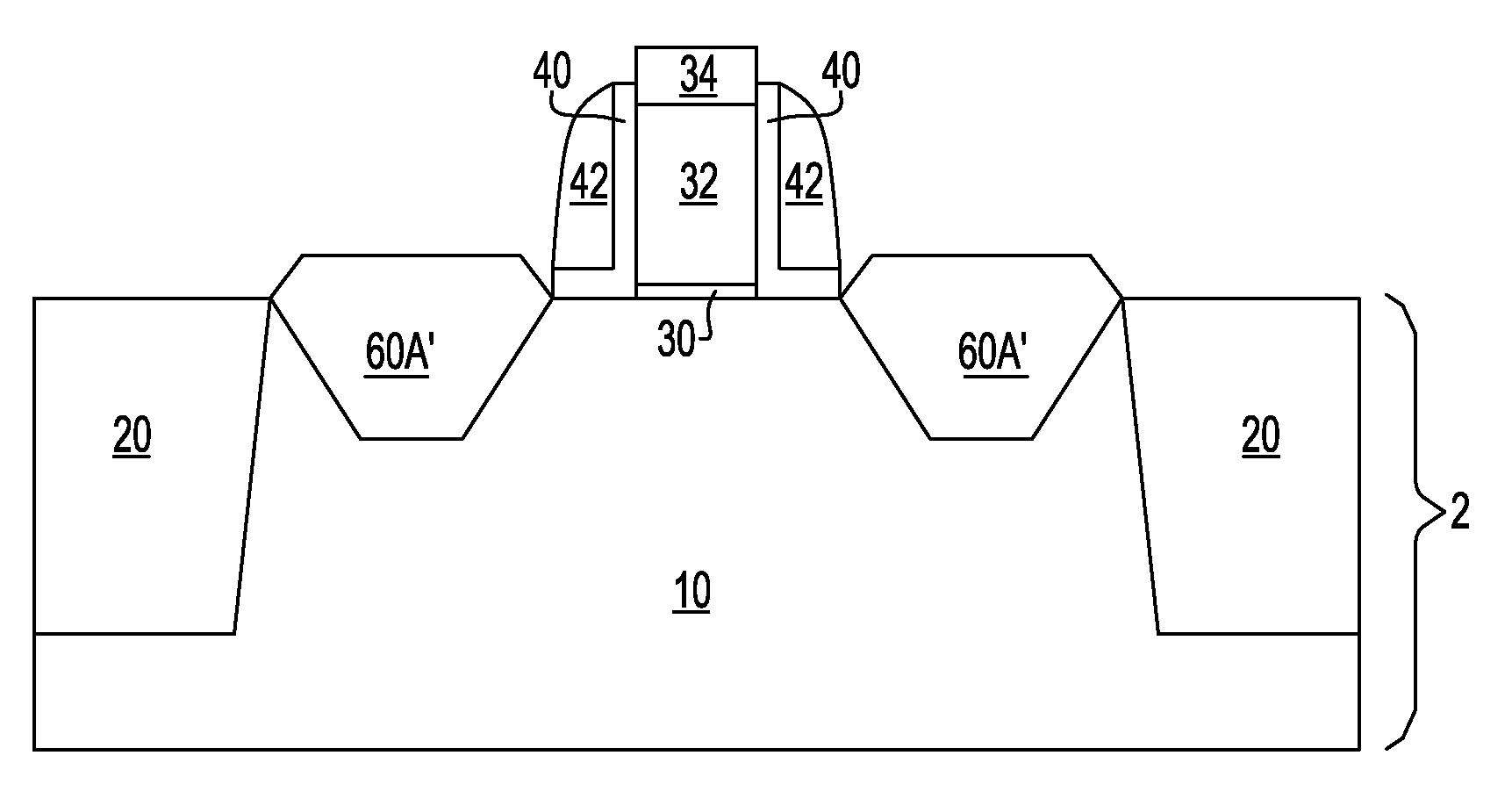
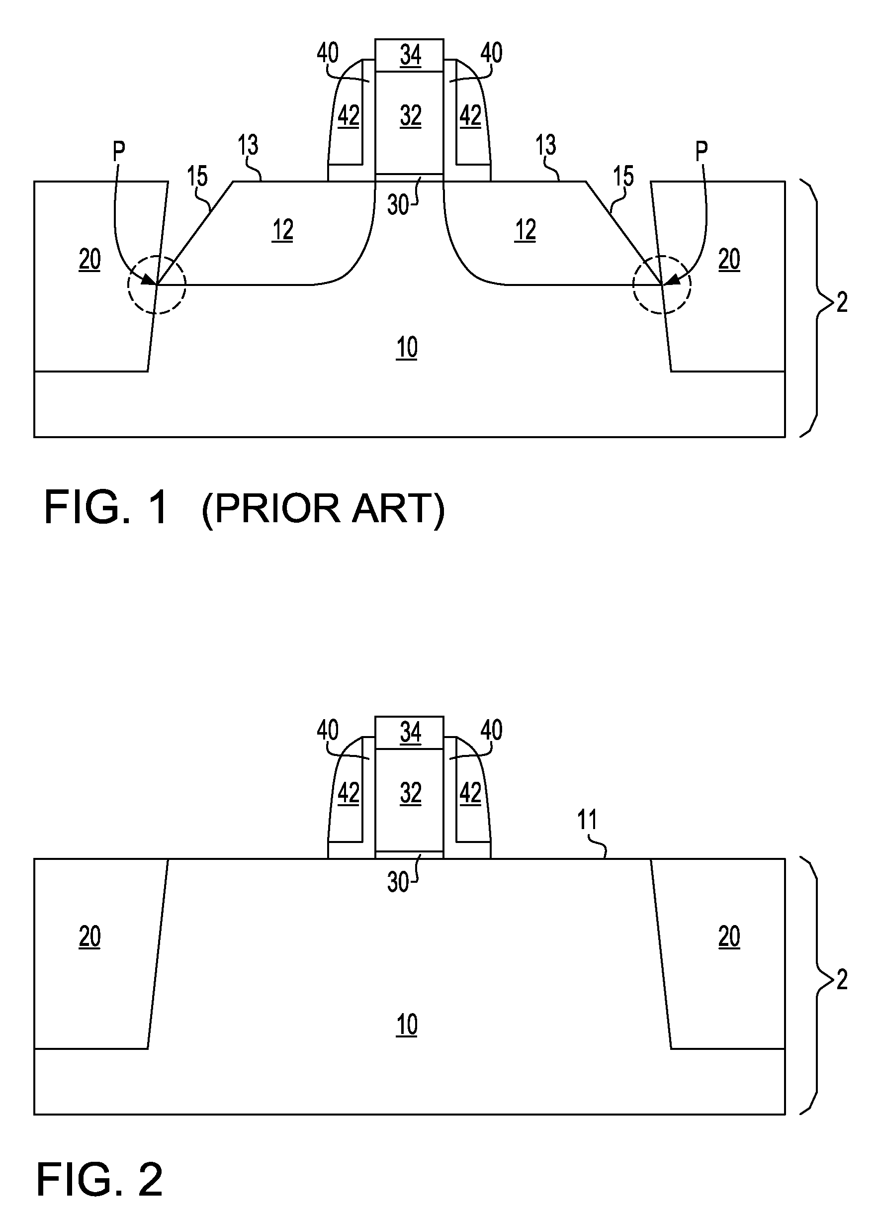
[0068]Referring to FIG. 9, a third exemplary structure according to the present invention is shown. The semiconductor structure in FIG. 8 is formed by subjecting the first exemplary semiconductor structure shown in FIG. 3 to a subsequent isotropic etch. During the isotropic etch, the substrate semiconductor material is removed at substantially the same rate along the various crystallographic orientations of the substrate semiconductor region 10. Preferably, the high etch rate crystallographic facets 50 are parallel to the original semiconductor surface 11. Alternatively, the high etch rate crystallographic facet 50 may not be parallel to the original semiconductor surface 11. The portions of the substrate semiconductor region 10 underneath the spacers (40, 42) are undercut during the isotropic etch. Further, the line at which a low etch rate crystallographic facet 51 adjoins the shallow trench isolation (STI) 20 is recessed downward along a sidewall of the STI 20. The cavity in the ...


PUM


Abstract

Source and drain regions of an FET are etched by a crystallographic anisotropic etch to form a cavity surrounded by crystallographic facets. The exposure of the sidewalls of shallow trench isolation (STI) is avoided or reduced compared to the prior art. The crystallographic anisotropic etch may be combined with an isotropic etch or a recess etch to create undercuts beneath gate spacers and/or a pegging line beneath a top surface of the STI. The at least one cavity is then filled with a lattice-mismatched embedded material so that stress is applied to the channel of the FET. The resulting structure has increased containment of the embedded semiconductor region by shallow trench isolation. A reduction in stress due to the unconstrained sidewall area and an increase in the junction current due to the recessing of the pegging line are eliminated or alleviated.

Description

FIELD OF THE INVENTION [0001]The present invention relates to semiconductor structures, and particularly, to semiconductor structures with at least one embedded semiconductor region and methods of manufacturing the same.BACKGROUND OF THE INVENTION [0002]Stress in the channel of a field effect transistor (FET) affects the on-current by altering the band structure of the semiconductor material, and consequently, the mobility of charge carriers. For example, the hole mobility of a p-type FET formed on a silicon substrate increases under a uniaxial compressive stress in the direction of the channel, i.e., along a line connecting the source and the drain. Similarly, the electron mobility of an n-type FET formed on a silicon substrate increases under a uniaxial tensile stress in the direction of the channel. The change in the mobility of minority carriers depends on the type and direction of stress as well as the semiconductor substrate material. By manipulating stress on the channel of a...

Claims


Application Information

Patent Timeline
Patent Type & Authority Applications(United States)
IPC IPC(8): H01L29/78
CPCH01L21/823412H01L21/823425H01L29/045H01L29/165H01L29/6656H01L29/66628H01L29/66636H01L29/7848
Inventor DYER, THOMAS W.CHIDAMBARRAO, DURESETI
Owner IBM CORP
Why Eureka
Try Eureka