Strained-channel transistor structure with lattice-mismatched zone

a strain-channel transistor and lattice-mismatched technology, applied in the direction of semiconductor devices, basic electric elements, electrical equipment, etc., can solve the problems of high defect density, difficult to achieve, and easy to strain relax

Inactive Publication Date: 2005-07-26
TAIWAN SEMICON MFG CO LTD
View PDF6 Cites 110 Cited by
  • Summary
  • Abstract
  • Description
  • Claims
  • Application Information

AI Technical Summary

Benefits of technology

[0010]Another object of the present invention is to provide a fabrication method of a strained-channel transistor structure.

Problems solved by technology

Therefore, there are some concerns about possible strain relaxation in the subsequent high temperature CMOS processes.
Further, the approach is very expensive since SiGe buffer layer 110 with thickness in the order of micrometers has to be grown.
Numerous dislocations exist in relaxed SiGe layer 114, some of which propagate to strained-Si layer 130, resulting in high defect density, thereby negatively affecting transistor performance.
However, uniaxial tensile strain in the source-to-drain degrades hole mobility while uniaxial compressive strain degrades electron mobility.
Ion implantation of germanium can be used to selectively relax the strain so that the hole or electron mobility is not degraded, but can be difficult to implement due to the close proximity of the N and P-channel transistors.

Method used


Image

  • Strained-channel transistor structure with lattice-mismatched zone
  • Strained-channel transistor structure with lattice-mismatched zone
  • Strained-channel transistor structure with lattice-mismatched zone

Examples


first embodiment

[0029

[0030]In the first embodiment of the present invention, two kinds of stress modes exerted on the strained-channel region according to the present invention are discussed.

[0031]In FIG. 3A, a cross section of a strained-channel transistor structure 3a in accordance with the first embodiment of the present invention is shown. Substrate 300a, having a strained channel region 306a in a surface, comprises a semiconductor material. Gate dielectric layer 312a, preferably with a thickness between about 3 and 100 Å, is on the strained channel region 306a. Gate electrode 314a is on the gate dielectric layer 312a. Spacer 316a is on a sidewall of gate electrode 314a and covers a part of the surface of substrate 300a. Drain region 307a, comprising drain extension region 301a and deeper drain region 302a, and source region 308a, comprising source extension region 303a and deeper source region 304a, are oppositely adjacent to strained channel region 306a. Lattice-mismatched zone 305a, comprisi...

second embodiment

[0036

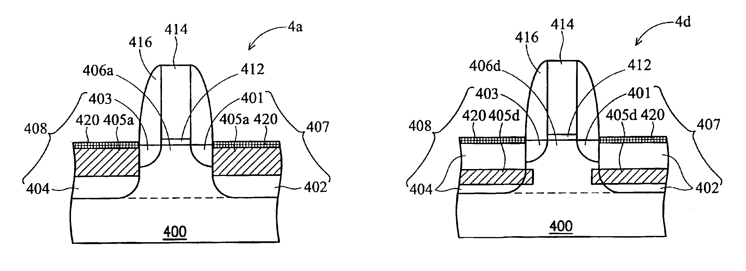
[0037]In the second embodiment of the present invention, different kinds of arrangements of lattice-mismatched zone in drain region and / or source region according to the present invention are discussed. In strained-channel transistor structures 4a through 4d in FIGS. 4A through 4D, relationships among substrate 400, drain extension region 401, deeper drain region 402, drain region 407, source extension region 403, deeper source region 404, source region 408, lattice-mismatched zone 405a / 405b / 405c / 405d, strained channel region 406a / 406b / 406c / 406d, gate dielectric layer 412, gate electrode 414, and spacer 416, the same as those described in the first embodiment of the present invention, are omitted.

[0038]In FIG. 4A, lattice-mismatched zone 405a is arranged near the surface of drain region 407 and / or source region 408, and does not extend into drain extension region 401 and / or source extension region 403. In FIG. 4B, lattice-mismatched zone 405b may protrude from the surface of dr...

third embodiment

[0041

[0042]In the third embodiment of the present invention, a fabrication method of a strained-channel transistor structure according to the present invention is described. A flowchart of the fabrication method in accordance with the third embodiment of the present invention is shown in FIG. 5. The subsequent descriptions of the fabrication method in accordance with the third embodiment of the present invention follow the steps in FIG. 5.

[0043]In FIG. 6A, a semiconductor substrate such as a silicon substrate 500 is provided. Silicon substrate 500 comprises a previously formed plurality of isolation regions (not shown) and previously defined plurality of device regions (not shown). For example, the isolation regions may be shallow trench isolation regions. FIGS. 6A through 6F provide a cross-sectional view of one single device region for easy description. Silicon substrate 500 comprises, a channel region 506 in an active surface. Silicon substrate 500 is N-type doped when strained-c...


PUM


Abstract

A strained-channel transistor structure with lattice-mismatched zone and fabrication method thereof. The transistor structure includes a substrate having a strained channel region, comprising a first semiconductor material with a first natural lattice constant, in a surface, a gate dielectric layer overlying the strained channel region, a gate electrode overlying the gate dielectric layer, and a source region and drain region oppositely adjacent to the strained channel region, with one or both of the source region and drain region comprising a lattice-mismatched zone comprising a second semiconductor material with a second natural lattice constant different from the first natural lattice constant.

Description

BACKGROUND OF THE INVENTION[0001]1. Field of the Invention[0002]The present invention relates to a semiconductor device with lattice-mismatched zone and fabrication method thereof, and more specifically to a strained-channel transistor structure and fabrication method thereof.[0003]2. Description of the Related Art[0004]Size reduction of the metal-oxide-semiconductor field-effect transistor (MOSFET), including reduction of gate length and gate oxide thickness, has enabled a continuous improvement in speed performance, density, and cost per unit function of integrated circuits during the past few decades.[0005]In order to further enhance performance of the transistor, strain may be introduced in the transistor channel to improve carrier mobility to enhance performance of the transistor in addition to device scaling. There are several existing approaches to introducing strain in a channel region of the transistor.[0006]In one conventional approach, as described in a paper titled “NMOS...

Claims


Application Information

Patent Timeline
Patent Type & Authority Patents(United States)
IPC IPC(8): H01L21/336H01L29/78H01L21/02H01L29/66H01L29/51H01L29/40H01L21/20H01L21/28
CPCH01L21/28194H01L29/7848H01L29/66628H01L29/66636H01L29/7834H01L29/7842H01L21/28202H01L21/28211H01L29/165H01L29/51H01L29/518H01L29/517
Inventor YEO, YEE-CHIALIN, CHUN-CHIEHLEE, WEN-CHINHU, CHENMING
Owner TAIWAN SEMICON MFG CO LTD
Why Eureka
Try Eureka