Semiconductor device
a technology of a semiconductor and a gate electrode, which is applied in the direction of semiconductor devices, electrical devices, transistors, etc., can solve the problems of difficult integral disadvantageous adjustment of the threshold of the gate electrode of the pmos circuit in the n-well, and complicating the layout of the interconnection, so as to achieve the effect of suppressing the propagation of nois
- Summary
- Abstract
- Description
- Claims
- Application Information
AI Technical Summary
Benefits of technology
Problems solved by technology
Method used
Image

Examples
first embodiment
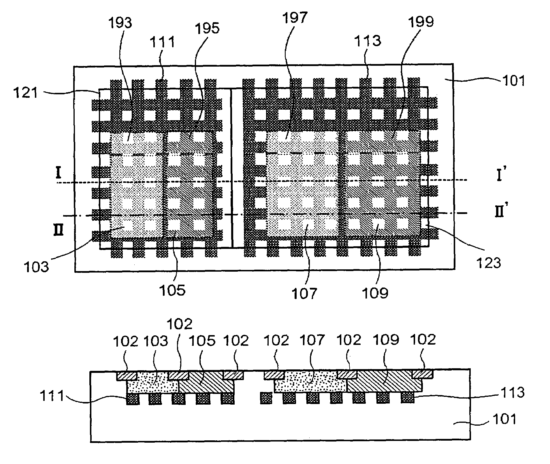
[0050]FIGS. 1A, 1B, and 1C are a plan view and cross-sectional views for describing a configuration of a semiconductor device according to the present invention. Although circuits configured by elements including a MOS transistor are actually provided in the semiconductor device shown in FIGS. 1A to 1C, they are not shown for convenience of illustration.
[0051]FIG. 1A is a plan view for describing the configuration of the semiconductor device according to this embodiment. The semiconductor device according to the first embodiment includes a P—Si substrate 101 (a semiconductor substrate of one-conductivity-type). In addition, a digital circuit region 123 and an analog circuit region 121 (a plurality of transistor formation regions) are formed on the P—Si substrate 101.
[0052]The analog circuit region 121 and the digital circuit region 123 include P-wells 103 and 193 and P-wells 107 and 197 (first regions of one-conductivity-type), respectively, which are formed at an element formation ...
second embodiment
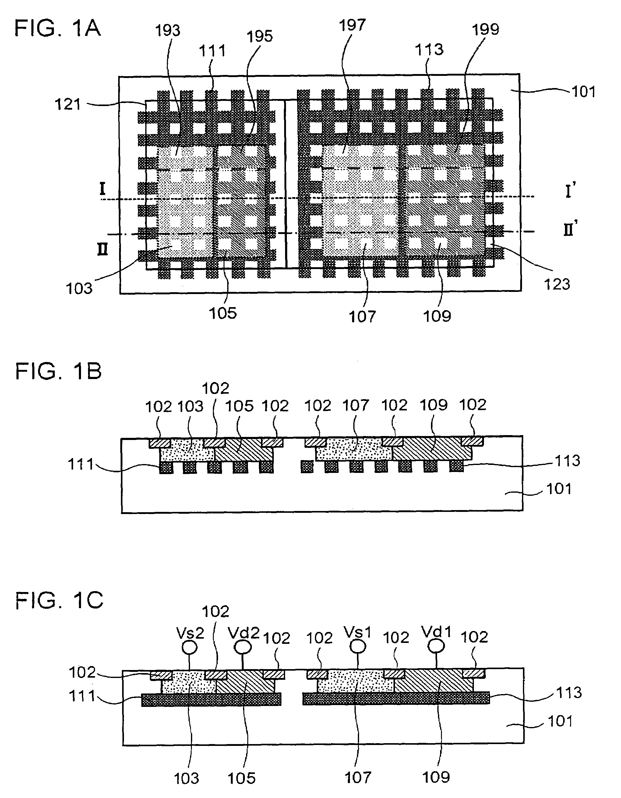
[0092]FIG. 2 is a plan view that typically depicts a configuration of a semiconductor device according to the present invention.
[0093]The configuration of a semiconductor device 200 according to the second embodiment is basically equal to that of the semiconductor device according to the first embodiment. The second embodiment differs from the first embodiment in arrangement of P-wells, N-wells, and deep N-wells. In this embodiment, the same configuration as that according to the first embodiment will not be described repeatedly.
[0094]The semiconductor device 200 according to this embodiment is configured so that N-wells 203a, 203b, 203c, 203d, 205, 207a, 207b, 207c, and 209 (second regions of an opposite conduction type) are provided at an element formation surface of a P—Si substrate 201. A square lattice-type deep N-well 211 is provided to contact with lower surfaces of the N-wells 203a, 203b, 203c, and 203d. A square lattice-type deep N-well 213 is provided to contact with a low...
third embodiment
[0100]FIG. 3 is a plan view that typically depicts a configuration of a semiconductor device according to the present invention.
[0101]The configuration of a semiconductor device 300 according to the third embodiment is basically equal to that of the semiconductor device according to the first embodiment. The third embodiment differs from the first embodiment in arrangement of P-wells, N-wells, and deep N-wells. In this embodiment, the same configuration as that according to the first embodiment will not be described repeatedly.
[0102]The semiconductor device 300 according to this embodiment is configured so that N-wells 303a, 303b, 303c, 303d, 305, 307a, 307b, 307c, and 309 are provided at an element formation surface of a P—Si substrate 301. An oblique lattice-type deep N-well 311 is provided to contact with lower surfaces of the N-wells 303a, 303b, 303c, and 303d. An oblique lattice-type deep N-well 313 is provided to contact with a lower surface of the N-well 305. An oblique latti...
PUM
 Abstract
Description
Claims
Application Information
 - R&D
- Intellectual Property
- Life Sciences
- Materials
- Tech Scout
- Unparalleled Data Quality
- Higher Quality Content
- 60% Fewer Hallucinations
Browse by: Latest US Patents, China's latest patents, Technical Efficacy Thesaurus, Application Domain, Technology Topic, Popular Technical Reports.
© 2025 PatSnap. All rights reserved.Legal|Privacy policy|Modern Slavery Act Transparency Statement|Sitemap|About US| Contact US: help@patsnap.com