
Semiconductor module and mobile apparatus

A semiconductor and conductor part technology, applied in the direction of semiconductor devices, semiconductor/solid-state device components, electric solid-state devices, etc., can solve the problem of inability to effectively suppress noise of circuit components, and achieve the effect of improving reliability

Inactive Publication Date: 2011-08-03
SANYO ELECTRIC CO LTD
View PDF3 Cites 2 Cited by
  • Summary
  • Abstract
  • Description
  • Claims
  • Application Information

AI Technical Summary

Problems solved by technology

[0006] In addition, in the method disclosed in Patent Document 2, although it is effective to place circuit elements having a digital circuit and circuit elements having an analog circuit on the same plane, even if a circuit element with an antenna is provided on the outer edge The multi-level stack structure formed by stacking layers still cannot effectively suppress the noise in the vertical direction between circuit elements

Method used


Image

  • Semiconductor module and mobile apparatus
  • Semiconductor module and mobile apparatus
  • Semiconductor module and mobile apparatus

Examples


no. 1 Embodiment approach

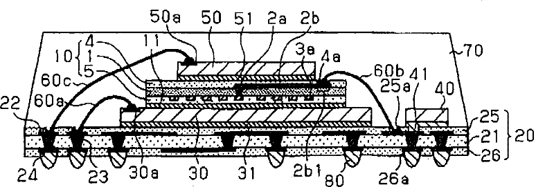
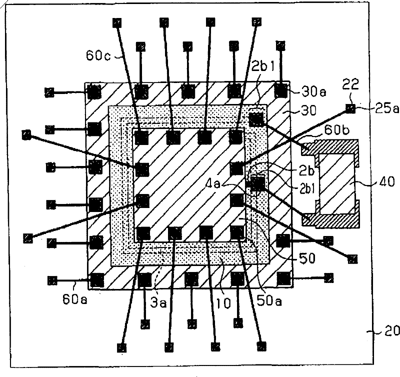
[0047] figure 1 is a cross-sectional view showing the structure of the semiconductor module of the first embodiment, figure 2 It is a plan view (top view) of the semiconductor module of the first embodiment. The semiconductor module of the first embodiment includes: a multilayer substrate 20; a first circuit element 30 mounted on the multilayer substrate 20; a second circuit element 50 stacked on the first circuit element 30; The interposer substrate 10 including the antenna conductor part 3a between the circuit element 30 and the second circuit element 50; the passive element 40 mounted on the multilayer substrate 20 and connected to the antenna conductor part 3a; the seal for sealing each element resin layer 70 .

[0048] The multilayer substrate 20 is, for example, a base substrate with a two-layer wiring structure, and has a wiring layer 22 and a wiring layer 24 on its upper and lower surfaces, respectively, with an insulating layer 21 interposed therebetween. The wiri...

no. 2 Embodiment approach

[0091] Figure 9 It is a design drawing of the antenna conductor part of the interposer board|substrate of 2nd Embodiment. The difference from the first embodiment is that the antenna conductor portion 3a1 of the interposer board 10 is changed from a spiral-shaped wiring pattern to a meander-shaped (Miander-shaped) wiring pattern. Here, the outer edge (dimension) of the antenna conductor portion 3a1 is the same as that of the first embodiment, and the outer edge of the common area (area within the dotted line) S where the first circuit element 30 and the second circuit element 50 overlap is viewed from above. (Size) is large, and the antenna conductor part 3a1 overlaps so that the whole common area S may be covered. Other than that, it is the same as the above-mentioned first embodiment. In addition, the antenna conductor part 3a1 is an example of the "conductor part" of this invention.

[0092] The interposer board 10 having such an antenna conductor portion 3a can be form...

no. 3 Embodiment approach

[0097] Figure 10 It is a design drawing of the antenna conductor part of the interposer board|substrate of 3rd Embodiment. The difference from the first embodiment is that the antenna conductor portion 3a2 of the interposer board 10 partially includes at least one of the first circuit element 30 and the second circuit element 50 in the common area S and becomes a source of noise. circuit area ( Figure 10 The area enclosed by the dotted line) overlaps the configuration in a selective coverage manner. Other than that, it is the same as the above-mentioned first embodiment. In addition, the antenna conductor part 3a2 is an example of the "conductor part" of this invention, and the circuit area N is an example of the "circuit area" of this invention.

[0098] Such an antenna conductor part 3a2 is in Figure 7 In the patterning step of the copper plating layer 3 shown in (F), it can be easily produced by changing its design.

[0099] According to the semiconductor module of ...


PUM


Abstract

The invention relates to a semiconductor module capable of effectively suppressing and reducing noise propagation between stacked circuit elements. The semiconductor module includes a first circuit element; a conductor, provided above the first circuit element, which functions as a loop antenna; and a second circuit element stacked above the conductor. By employing this embodiment, the antenna conductor, which functions as a loop antenna, is provided between the first circuit element and the second circuit element. The provision of this antenna conductor can shield noise propagation between the first circuit element and the second circuit element by absorbing it. This contributes to stabilizing the operation of the semiconductor module, thus improving the reliability thereof.

Description

technical field [0001] The present invention relates to a semiconductor module, and in particular, to a semiconductor module in which a plurality of circuit elements are laminated, and a portable device equipped with the semiconductor module. Background technique [0002] In recent years, a multi-stage stack structure (multi-chip package) in which a plurality of circuit elements are mixed and mounted by lamination has been known as a packaging technology for realizing miniaturization and high functionality of circuit devices used in electronic equipment. However, such a circuit device with a multi-stage stack structure has a problem that, for example, when circuit elements formed with analog circuits and circuit elements formed with digital circuits are stacked and placed in a mixed manner, the high-speed operation of digital circuits may be difficult. High-frequency noise (noise having a high-frequency component) generated on circuit elements propagates to circuit elements ...

Claims


Application Information

Patent Timeline
Patent Type & Authority Patents(China)
IPC IPC(8): H01L25/00H01L23/552H01L23/48
CPCH01L2924/15311H01L2224/48091H01L2224/73265H01L2224/48465H01L2924/30107H01L2924/3025
Inventor 今冈俊一大塚健志泽井彻郎
Owner SANYO ELECTRIC CO LTD
Learn More