Semiconductor device with noise control

a semiconductor device and noise control technology, applied in semiconductor devices, semiconductor/solid-state device details, electrical equipment, etc., can solve problems such as operation errors, power supply/ground wiring noise current generation, operation errors, etc., to prevent operation errors, suppress noise propagation, and reduce radiation noise

Inactive Publication Date: 2008-08-05
CANON KK
View PDF8 Cites 2 Cited by
  • Summary
  • Abstract
  • Description
  • Claims
  • Application Information

AI Technical Summary

Benefits of technology

[0011]The present invention has been made in consideration of the above-described problems, and has as its object to reduce radiation noise and prevent any operation error by suppressing noise propagation between an input / output circuit and an internal circuit while preventing or minimizing an increase in the number of steps of semiconductor element design.
[0014]According to the present invention, radiation noise can be reduced, and any operation error can be prevented by suppressing noise propagation between an input / output circuit and an internal circuit while preventing or minimizing an increase in labor of semiconductor element design.

Problems solved by technology

In the above-described structure, a noise current which is generated in the power supply / ground wiring in the semiconductor device when it operates poses a problem.
As a result, the potential immediately under the channel of the MOS transistor varies and causes an operation error.
Another problem of noise is radiation noise which is generated when the noise current of the power supply / ground in the internal circuit region propagates to the input / output circuit region through the power supply / ground wiring, and the power supply / ground noise of the internal circuit is superimposed on a signal of an input / output circuit, which is to be output to the outside.
However, there is no measure against noise propagation through the semiconductor substrate between the internal circuit and the input / output circuits at all.
Hence, the prior arts cannot prevent an operation error caused by propagation of noise, represented by SSN (Simultaneous Switching Noise) of the input / output circuits, which is generated by the input / output circuit operation to the internal circuit through the semiconductor substrate, or an increase in radiation noise caused by noise propagation from the internal circuit to the input / output circuits through the semiconductor substrate.

Method used


Image

  • Semiconductor device with noise control
  • Semiconductor device with noise control
  • Semiconductor device with noise control

Examples


first embodiment

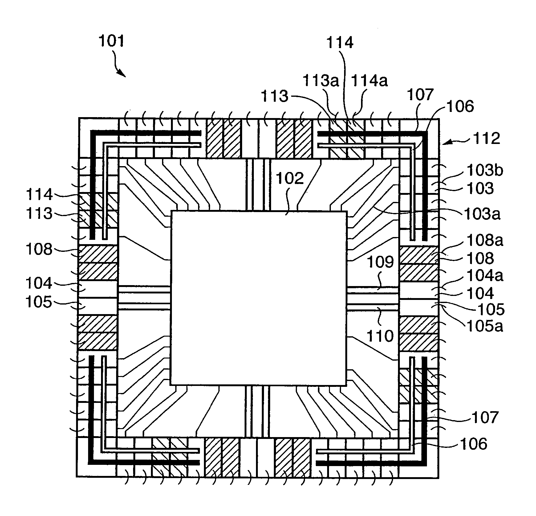
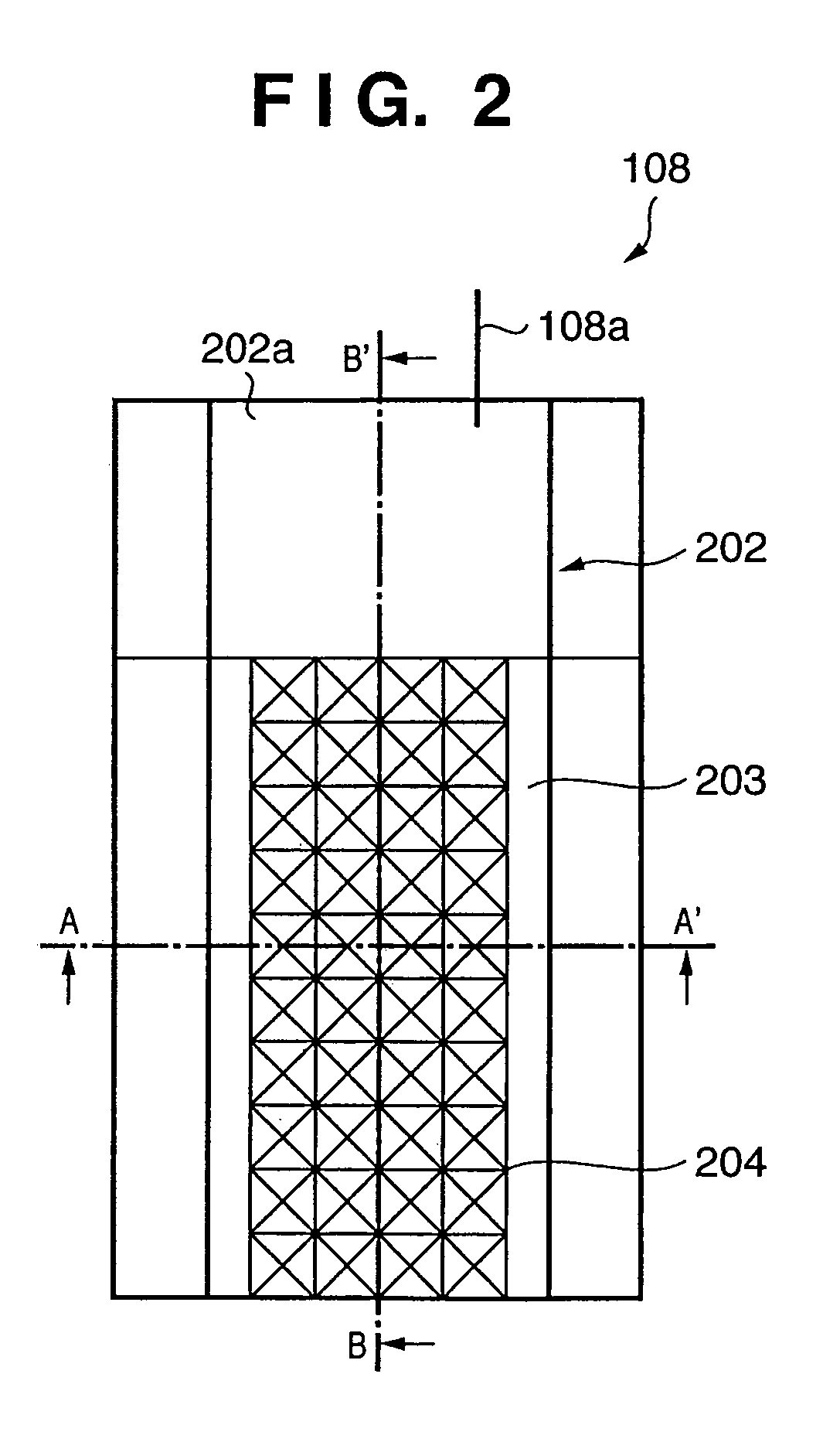
[0033]FIGS. 1, 2, 3, and 4 are views showing the first embodiment of the present invention. FIG. 1 is a view showing the outline of the layout of a semiconductor device according to the first embodiment. FIG. 1 corresponds to FIG. 16 which shows a prior art (to be described later). FIG. 2 shows the structure of a noise control cell 108 as a principal part of the first embodiment. FIGS. 3 and 4 are sectional views taken along a line A-A′ in FIG. 2. FIG. 5 is a sectional view of the noise control cell 108 taken along a line B-B′.

[0034]Referring to FIG. 1, a semiconductor device 101 comprises an internal circuit 102 and input / output circuit region 112. The input / output circuit region 112 comprises input / output cells (I / O cells) 103 which transmit signals between the internal circuit 102 and a device outside the semiconductor device 101, power supply wiring 107 and ground wiring 106 to supply a power and ground to the input / output cells 103, input / output circuit power supply cells 113 t...

second embodiment

[0046]FIGS. 6 to 13 show the second embodiment. The same reference numerals as in the first embodiment denote the same functional parts in the second embodiment, and a description thereof will be omitted.

[0047]The difference from the first embodiment is that extended noise control wiring 511 independently of input / output circuit power supply wiring 107 and ground wiring 106 and internal circuit power supply wiring 109 and ground wiring 110 are present in an input / output circuit region 512, the extended noise control wiring 511 automatically connect noise control cells 508 when normal input / output cells 503 and the noise control cells 508 are arranged, and the extended noise control wiring 511 are connected to the semiconductor substrate through contact vias. The noise control cell 508 has almost the same function as the noise control cell 108 of the first embodiment.

[0048]In the first embodiment, power supply noise and ground noise generated by the internal circuit operation are abs...

third embodiment

[0058]FIG. 15 shows the third embodiment.

[0059]In this embodiment, the same input / output cells as in the first embodiment are used, and the semiconductor layout designer connects noise control cells 108 by wiring 1211. The wiring 1211 is connected to the semiconductor substrate. The semiconductor device designer connects the wiring 1211 to the semiconductor substrate arbitrarily by using wiring, vias, p+-, or n+-regions, as shown in FIG. 8, 9, 10, or 11.

[0060]As in the second embodiment, the noise absorption effect of the first embodiment can be increased. According to this embodiment, the noise control cells 108 are arbitrarily connected by the wiring 1211 only at a portion where noise propagation should be prevented. Hence, the area utilization ratio of the semiconductor device can be increased as compared to the structure of the second embodiment in which the noise control cells are always connected.

[0061]As described above, according to the above-described embodiment, the noise ...


PUM


Abstract

Radiation noise is reduced, and any operation error is prevented by suppressing noise propagation between an input / output circuit and an internal circuit while preventing or minimizing an increase in the number of steps of semiconductor element design. A semiconductor device having an input / output circuit region and an internal circuit region includes an internal circuit power supply cell which is arranged in the input / output circuit region and supplies a power to the internal circuit region, an internal circuit ground cell which is arranged in the input / output circuit region and supplies ground to the internal circuit region, and noise control cells which are arranged to sandwich the internal circuit power supply cell and the internal circuit ground cell in the input / output circuit region and formed by electrically connecting a p-type semiconductor substrate to ground independently of the input / output circuit region and the internal circuit region.

Description

FIELD OF THE INVENTION[0001]The present invention relates to a noise control technique of a semiconductor device.BACKGROUND OF THE INVENTION[0002]A semiconductor device represented by an ASIC (Application Specific Integrated Circuit) normally has an internal circuit region and an input / output circuit region arranged around it. A circuit having a desired function such as signal processing is formed in the internal circuit region. This circuit is formed by arranging a plurality of cells using a plurality of semiconductor elements such as MOS transistors (Metal Oxide Semiconductor transistors) and connecting them by wiring.[0003]The input / output circuit region transmits signals between the internal circuit region and a device outside the semiconductor device or supplies a power and reference potential (to be referred to as ground hereinafter) necessary for the ground in the internal circuit region and input / output circuit region to operate. The signals and power supply / ground in the in...

Claims


Application Information

Patent Timeline
Patent Type & Authority Patents(United States)
IPC IPC(8): H01L31/112
CPCH01L23/5286H01L27/118H01L27/11898H01L24/06H01L2924/1301H01L2924/13091H01L2924/00H01L2924/14
Inventor HOSHI, SOU
Owner CANON KK
Why Eureka
Try Eureka