Electronic component and electronic component module

a technology of electronic components and electronic components, applied in the direction of lasers, basic electric elements, semiconductor lasers, etc., can solve the problems of optical communication module error or component breakdown, and achieve the effect of limiting noise transmission

Inactive Publication Date: 2010-02-16
SUMITOMO ELECTRIC DEVICE INNOVATIONS
View PDF3 Cites 2 Cited by
  • Summary
  • Abstract
  • Description
  • Claims
  • Application Information

AI Technical Summary

Benefits of technology

[0010]With the above-mentioned configuration, it is possible to limit a noise transmission from the first base portion to outside, because the first base portion is insulated from the second base portion with the insulator. It is possible to limit a transmission of an external signal to the first base portion. Accordingly, the electronic component is less subjected to a noise with other components.
[0012]With the above-mentioned configuration, it is possible to limit a noise transmission from the first base portion to outside through the module unit, because the first base portion is insulated from the second base portion with the insulator. It is possible to limit a transmission of an external signal to the first base portion through the module unit. Accordingly, the electronic component module is less subjected to a noise with other components.

Problems solved by technology

The noise causes error of the optical communication module or breakdown of the components.

Method used


Image

  • Electronic component and electronic component module
  • Electronic component and electronic component module
  • Electronic component and electronic component module

Examples


first embodiment

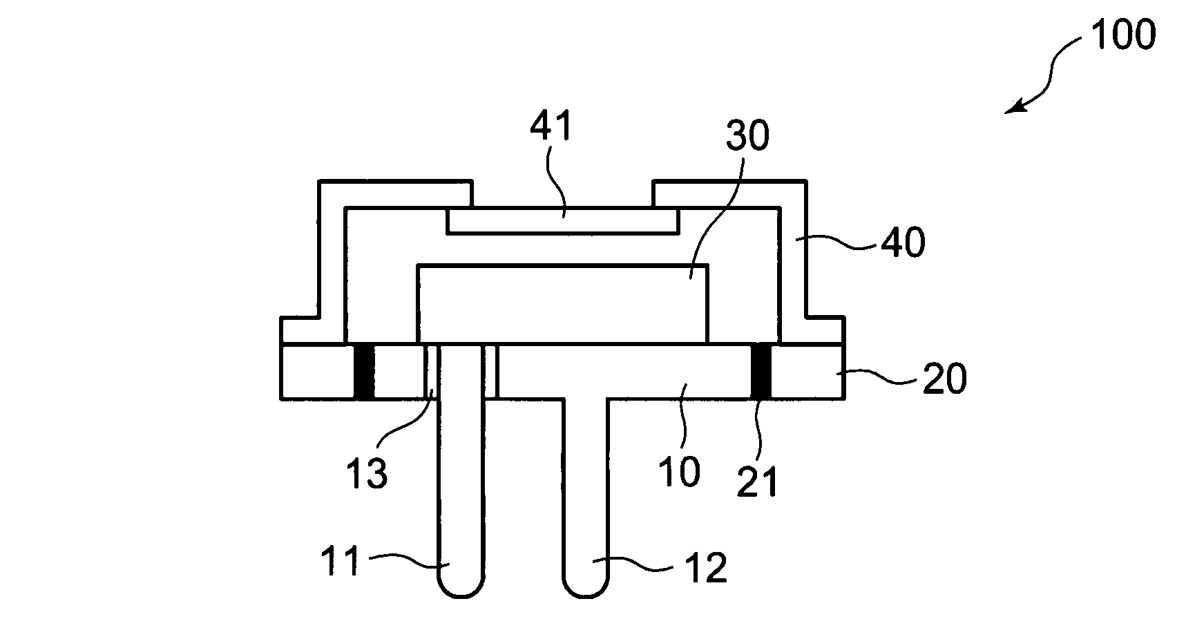
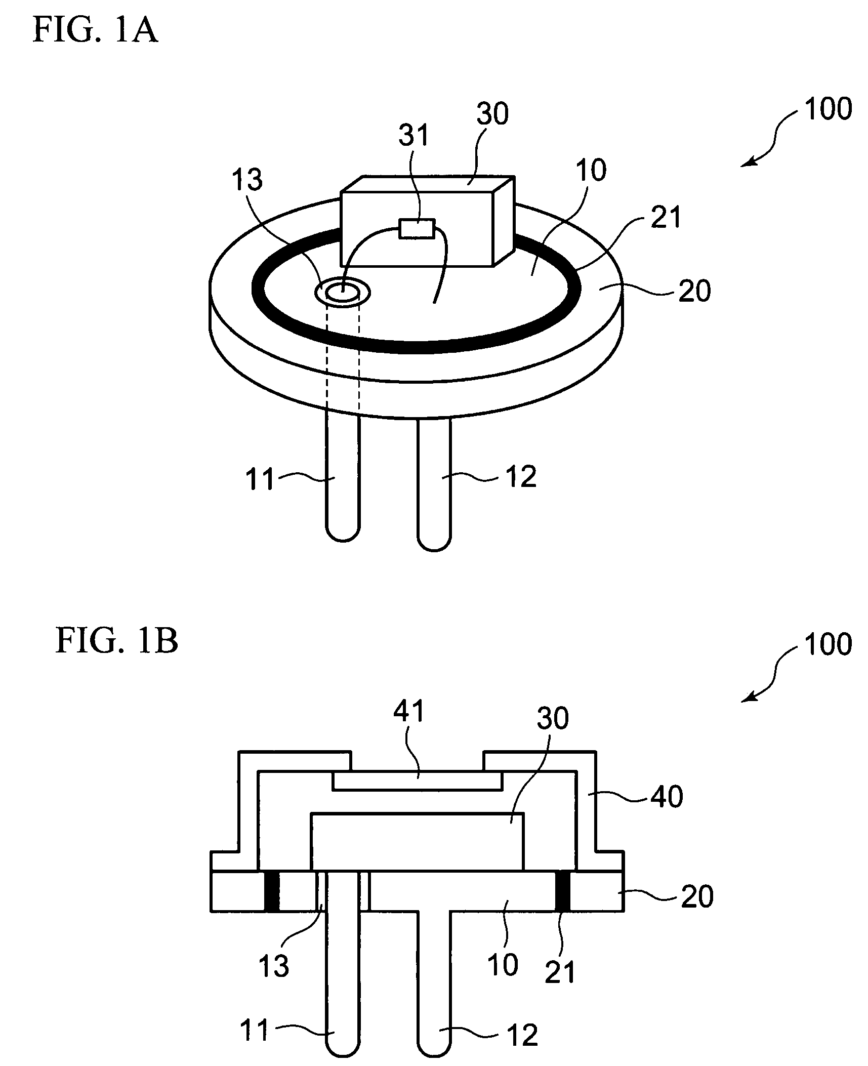
[0019]FIG. 1A and FIG. 1B illustrate an electronic component 100 in accordance with a first embodiment of the present invention. FIG. 1A illustrates a perspective view of the electronic component 100. FIG. 1B illustrates a cross sectional view of the electronic component 100. As shown in FIG. 1A and FIG. 1B, the electronic component 100 has a first base portion 10, a second base portion 20, an electronic element mounting portion 30 and a cap 40. In FIG. 1A, the cap 40 is omitted.

[0020]The first base portion 10 is a metal member having a substantially disc shape. A lead 11 and a lead 12 are provided on the first base portion 10. The lead 11 is a terminal where a signal is provided, and passes through the first base portion 10. The lead 12 is a terminal at ground potential, and is fixed to the first base portion 10. A lead-holding portion 13 is provided between the first base portion 10 and the lead 11. The lead-holding portion 13 has an insulating property. Accordingly, the first bas...

second embodiment

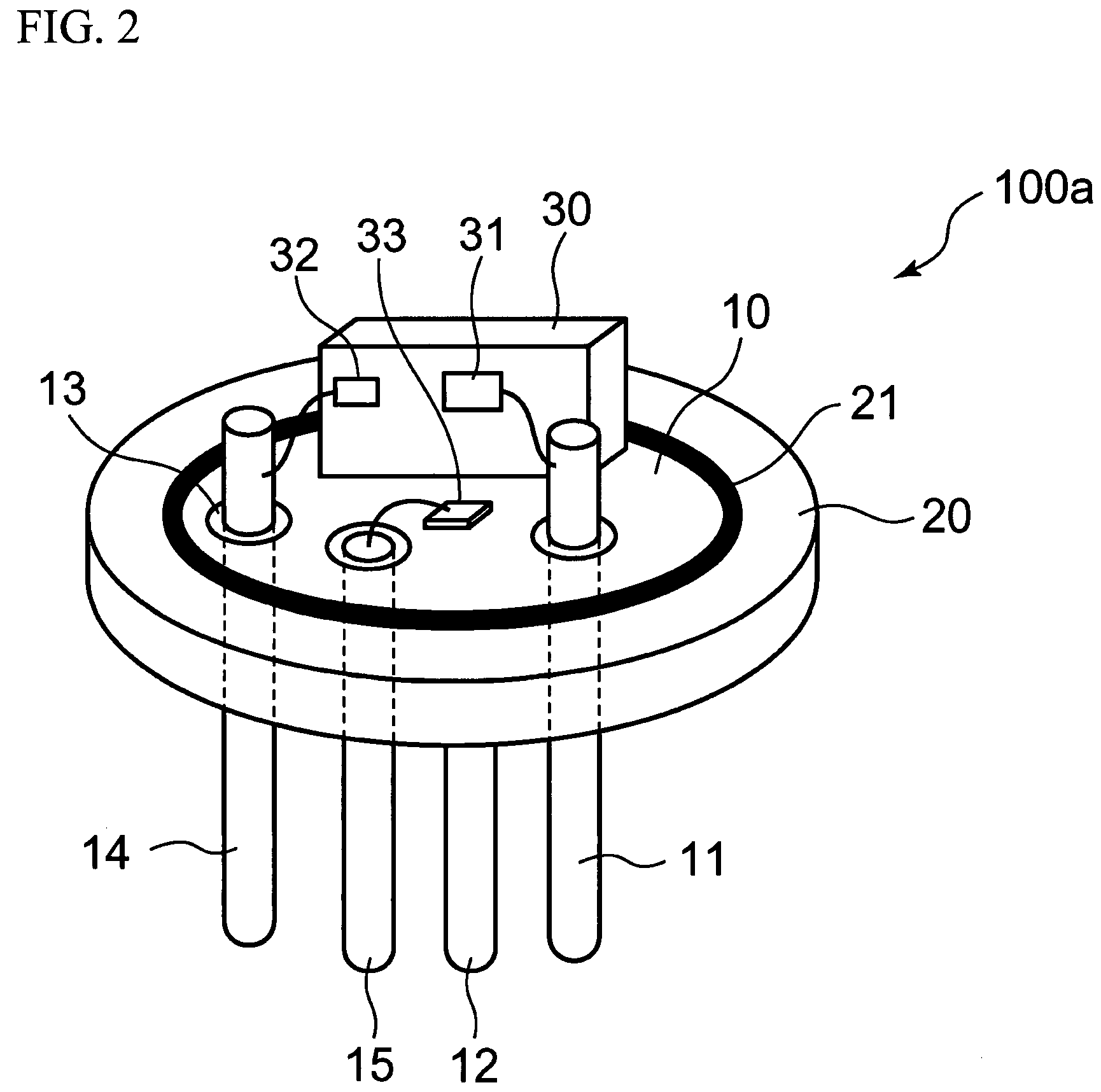
[0026]Next, a description will be given of an electronic component 100a in accordance with a second embodiment of the present invention. FIG. 2 illustrates a perspective view of the electronic component 100a . As shown in FIG. 2, the electronic component 100a has further a temperature sensor 32, a photo diode 33 and leads 14 and 15, being different from the electronic component 100 shown in FIG. 1. The same components have the same reference numerals in order to avoid a duplicated explanation. In FIG. 2, the cap 40 is omitted.

[0027]The leads 14 and 15 pass through the first base portion 10. The lead-holding portion 13 is provided between the first base portion 10 and the leads 14 and 15. Therefore, the leads 14 and 15 are electrically insulated from the first base portion 10, and the lead 14 is electrically insulated from the lead 15. The temperature sensor 32 is mounted on the electronic element mounting portion 30. The temperature sensor 32 detects a temperature of the laser diode...

third embodiment

[0030]Next, a description will be given of an optical communication module 200 in accordance with a third embodiment of the present invention. Generally, an optical communication module has an optical communication device and a module unit. The module unit has an optical component such as a lens holder having a lens, a guide fixing a package, a fixing member such as a fixing portion of an optical component.

[0031]FIG. 3 illustrates a cross sectional view of the optical communication module 200. As shown in FIG. 3, the optical communication module 200 has the electronic component 100 shown in FIG. 1, a lens holder 50, a fixing portion 60, a guide 61, a fiber-holding member 62 and a fiber 63. The fixing portion 60 is a metal member for fixing the lens holder 50. A lower end of the fixing portion 60 is fixed only to the second base portion 20 without contacting to the first base portion 10. An upper end of the fixing portion 60 is coupled to the lens holder 50.

[0032]The lens holder 50 i...


PUM


Abstract

An electronic component includes an electronic element, a conductive first base portion, a conductive second base portion, an insulator and a terminal. An electronic element is to be mounted on the electronic element mounting portion. The electronic element mounting portion is mounted on the first base portion. The insulator insulates the first base portion from the second base portion and couples the first base portion to the second base portion. The terminal is provided on the first base portion and is insulated from the first base portion.

Description

BACKGROUND OF THE INVENTION[0001]1. Field of the Invention[0002]This invention generally relates to an electronic component and an electronic component module.[0003]2. Description of the Related Art[0004]An electronic component for optical communication, in which a laser diode chip is mounted in a cylindrical case, is developed. The electronic component for the optical communication has a structure in which a laser diode, a laser-diode-mounting portion, a photo diode detecting an output light from the laser diode and so on are mounted on a metal base. Generally, these components are covered with a metal cap and the cap is fixed to the base.[0005]A lead, a ground terminal and so on are coupled to the base. The lead couples the mounted components to an external component electrically. Japanese Patent Application Publication No. 5-95169 discloses an optical communication module in which the electronic components and metal components such as a lens holder, a lens guide or the like are c...

Claims


Application Information

Patent Timeline
Patent Type & Authority Patents(United States)
IPC IPC(8): H01L23/043H01L23/00H01L23/02H01L23/04H01S5/022
CPCH01S5/02212H01L23/552H01L33/483H01S5/02276H01S5/02284H01S5/0683H01L2924/3025H01L2224/48091H01L2924/00014H01L2924/00H01S5/02345H01S5/02251
Inventor TATEIWA, YOSHIHIRONAKAGAWA, KAKUSHI
Owner SUMITOMO ELECTRIC DEVICE INNOVATIONS
Why Eureka
Try Eureka