Metal foil-clad substrate, circuit board and electronic-component mounting substrate

A technology for circuit substrates and electronic components, applied in the direction of circuit substrate materials, printed circuit components, three-dimensional rigid printed circuit boards, etc., can solve the problems of time and energy required for prepreg manufacturing, and achieve the effect of preventing the spread of noise

Inactive Publication Date: 2016-02-10
SUMITOMO BAKELITE CO LTD
View PDF1 Cites 1 Cited by
  • Summary
  • Abstract
  • Description
  • Claims
  • Application Information

AI Technical Summary

Problems solved by technology

[0006] However, in the manufacturing method using such a lamination method, there are problems in that a large-scale device such as a vacuum lamination device and a hot air drying device is required, and time and effort are required to manufacture the prepreg.

Method used


Image

  • Metal foil-clad substrate, circuit board and electronic-component mounting substrate
  • Metal foil-clad substrate, circuit board and electronic-component mounting substrate
  • Metal foil-clad substrate, circuit board and electronic-component mounting substrate

Examples


no. 1 Embodiment approach >

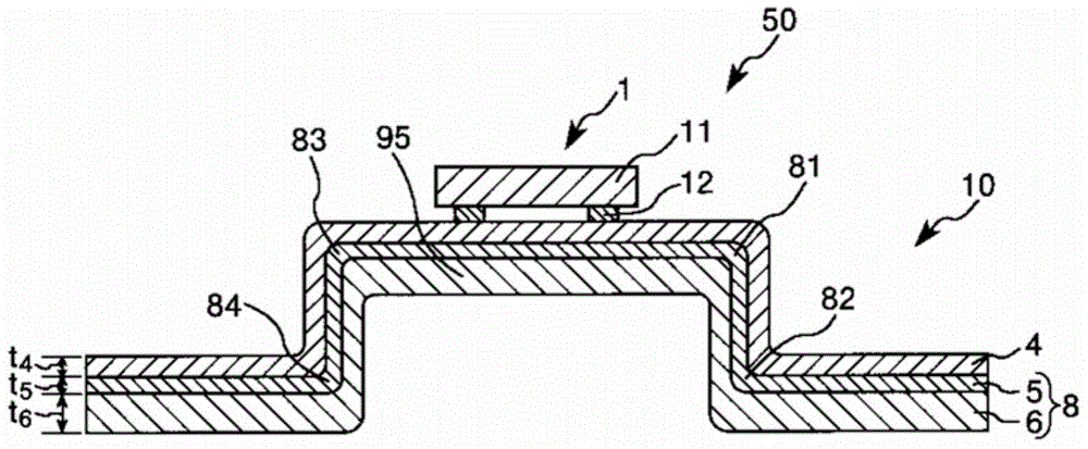
[0050] figure 1 It is a longitudinal sectional view showing the first embodiment of the electronic component mounting substrate of the present invention. It should be explained that in the following, for the convenience of explanation, the figure 1 The upper side in is referred to as "upper", and the figure 1 The lower side in is called "lower", and the figure 1 The right side in is called "Right", and the figure 1 The left side in is called "Left". In addition, each figure shows an exaggerated schematic diagram of an electronic component mounting board and its respective parts, and the sizes and ratios of the electronic component mounting board and its respective parts are greatly different from actual ones.

[0051] figure 1 The illustrated electronic component mounting board 50 has a semiconductor device 1 as an electronic component and a circuit board (circuit board of the present invention) 10 on which the semiconductor device 1 is mounted. It should be noted that, ...

no. 2 Embodiment approach >

[0234] Next, a second embodiment of the electronic component mounting substrate of the present invention will be described.

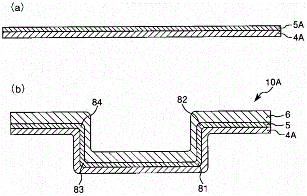
[0235] Figure 4 It is a vertical cross-sectional view showing a second embodiment of the electronic component mounting substrate of the present invention.

[0236] Hereinafter, the electronic component mounting board 51 of the second embodiment will be described focusing on differences from the electronic component mounting board 50 of the first embodiment described above, and the description of the same matters will be omitted.

[0237] Figure 4 The illustrated electronic component mounting board 51 mounts the semiconductor device 1 on the upper surface of a circuit board 10a having a configuration different from that of the circuit board 10 of the first embodiment, and is similar to figure 1 The illustrated electronic component mounting substrate 50 is the same.

[0238] That is, in the electronic component mounting board 51 according to the seco...

no. 3 Embodiment approach >

[0241] Next, a third embodiment of the electronic component mounting substrate of the present invention will be described.

[0242] Figure 5 It is a vertical cross-sectional view showing a third embodiment of the electronic component mounting substrate of the present invention.

[0243] Hereinafter, the electronic component mounting board 52 of the third embodiment will be described focusing on differences from the electronic component mounting board 50 of the first embodiment described above, and the description of the same matters will be omitted.

[0244] Figure 5 The illustrated electronic component mounting board 52 mounts the semiconductor device 1 on the upper surface of the circuit board 10 b having a configuration different from that of the circuit board 10 of the first embodiment, and is similar to figure 1 The illustrated electronic component mounting substrate 50 is the same.

[0245] That is, in the electronic component mounting board 52 according to the thir...


PUM

PropertyMeasurementUnit
thermal conductivityaaaaaaaaaa
glass transition temperatureaaaaaaaaaa
storage modulusaaaaaaaaaa

Abstract

The invention provides a metal foil-clad substrate, a circuit board manufactured by using the substrate and an electronic component carrying substrate on which an electronic component is carried. The metal foil-clad substrate can be manufactured into a circuit board which does not cause restraint to the overall shape of another structural body and can be carried on the another structural body without a large-scale device and without costing much time and effort. The metal foil-clad substrate is used for forming a circuit board which carries an electronic component. The metal foil-clad substrate includes a metal foil, a resin layer formed on one surface of the metal foil, and an insulating part formed on a surface of the resin layer opposite to the metal foil; and at least one bending portion in which the metal foil, the resin layer and the insulating part are bended to a side of the metal foil or the insulating part. The resin layer is constituted of a cured material or solidified material of a second resin composition containing a resin material. The insulating part is constituted of a cured material of a first resin composition containing a first thermosetting resin.

Description

technical field [0001] The present invention relates to a metal foil-clad substrate, a circuit substrate, and an electronic component mounting substrate. Background technique [0002] In recent years, high-density integration and high-density mounting of electronic components included in the above-mentioned electronic equipment have progressed in response to demands for higher functionality of electronic equipment. As a printed wiring board on which these electronic components are mounted, a substrate that suppresses propagation of noise generated by driving the electronic components is required. [0003] As such a printed wiring board (circuit board), for example, Patent Document 1 discloses a printed wiring board manufactured as follows. First, a resin composition is impregnated into a fibrous base material made of glass fibers or the like. Thereafter, the resin composition is semi-cured to obtain a sheet-shaped prepreg including a fibrous base material and a resin layer...

Claims


Application Information

Patent Timeline
Patent Type & Authority Applications(China)
IPC IPC(8): H05K1/03H01L21/48H01L23/498
CPCH01L21/48H01L21/4846H01L23/498H01L23/49838H05K1/036H05K1/0373H05K2201/0145H05K2201/0209B32B15/08B32B27/20B32B27/38B32B2255/06B32B2255/26B32B2307/202B32B2307/304B32B2457/08H01L2224/16225H01L2224/48091H01L2924/181H05K1/0216H05K1/0243H05K1/0284H05K3/0014Y10T428/24628H01L2924/00012H01L2924/00014H05K2201/0215
Inventor 冈坂周小宫谷寿郎小泉浩二马场孝幸
Owner SUMITOMO BAKELITE CO LTD
Why Eureka
Try Eureka