Signal processing device, signal processing method, reception device, transmission/reception device, communication module, and electronic device

a signal processing and signal processing technology, applied in the direction of instruments, pulse techniques, code conversion, etc., can solve the problems of difficult circuit design, limited chip layout, and difficult to completely suppress the propagation of noise, so as to reduce the high-frequency noise

Inactive Publication Date: 2013-08-13
ORMON CORP
View PDF9 Cites 1 Cited by
  • Summary
  • Abstract
  • Description
  • Claims
  • Application Information

AI Technical Summary

Benefits of technology

[0012]Consideration is also made to separate the power supply line for the analog circuit and the digital circuit on the chip and on the package, or to separate the ground line for the analog circuit and for the digital circuit. However, the capacitive component and inductance component remain between the separated power supply lines, and similarly, the capacitive component and inductance component remain between the separated ground lines, and hence it is difficult to completely suppress the propagation of noise.
[0040]Therefore, the signal processing device according to one or more embodiments of the present invention performs amplification and cuts off the high-frequency component with respect to the inputted analog signal in the analog circuit unit thereby obtaining the effect of reducing the high-frequency noise mixed to the analog signal propagated from the digital circuit unit to the analog circuit unit, and performs conversion to a digital signal of a predetermined format and waveform rectification on the signal which is subjected to amplification and whose high-frequency component is cut off in the digital circuit unit thereby obtaining the effect in that the increase in power consumption can be suppressed compared to the case where the waveform is rectified in the analog circuit unit.

Problems solved by technology

In this case, however, the layout of the chip is limited, and the designing of the circuit becomes difficult.
However, the capacitive component and inductance component remain between the separated power supply lines, and similarly, the capacitive component and inductance component remain between the separated ground lines, and hence it is difficult to completely suppress the propagation of noise.
In this case, however, the layout of the chip is limited, and the designing of the circuit becomes difficult.
As described above, because it is difficult to completely avoid the propagation of noise from the digital circuit to the analog circuit, noise countermeasures for reducing the noise component mixed in the analog signal become necessary.

Method used


Image

  • Signal processing device, signal processing method, reception device, transmission/reception device, communication module, and electronic device
  • Signal processing device, signal processing method, reception device, transmission/reception device, communication module, and electronic device
  • Signal processing device, signal processing method, reception device, transmission/reception device, communication module, and electronic device

Examples


first embodiment

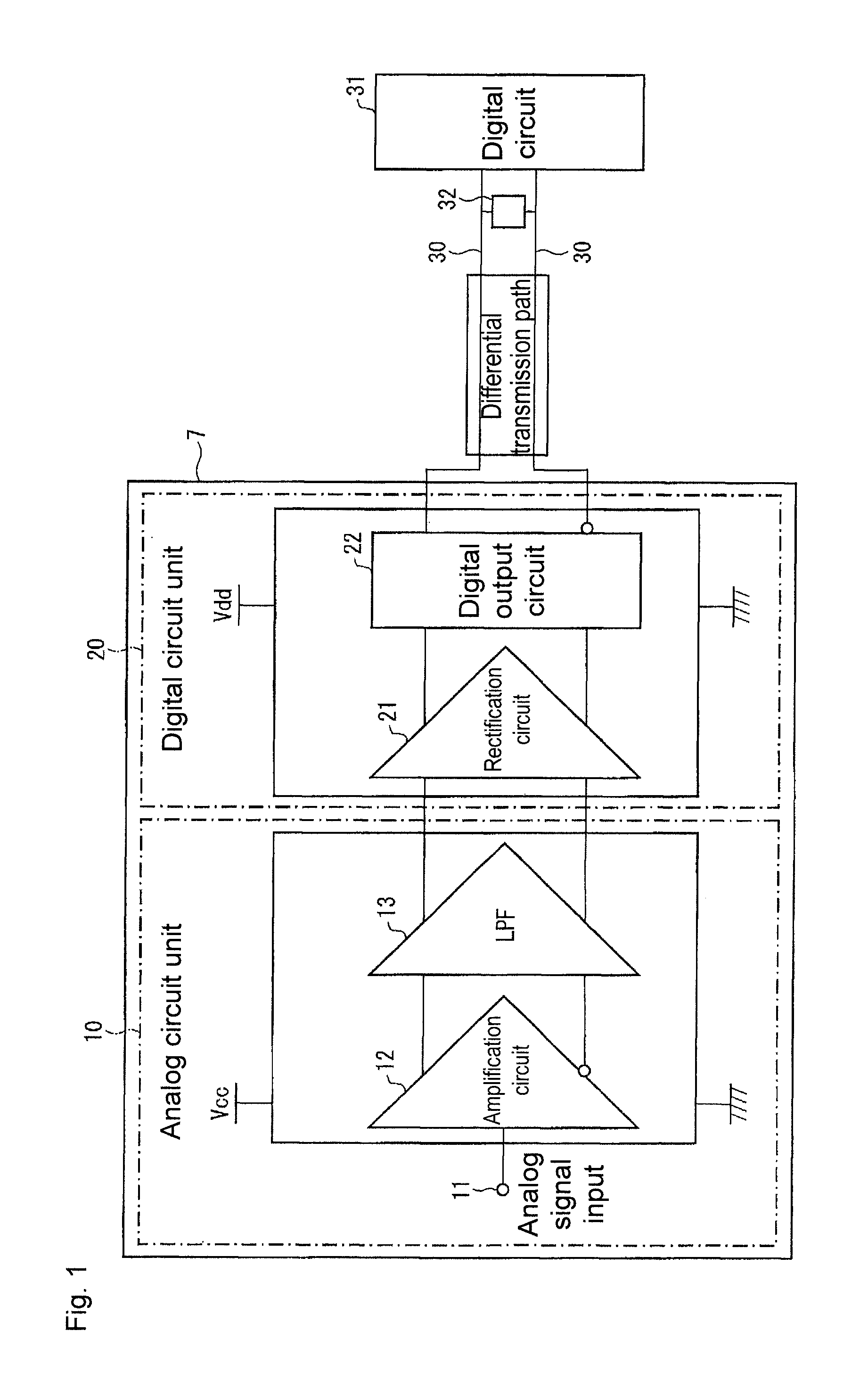
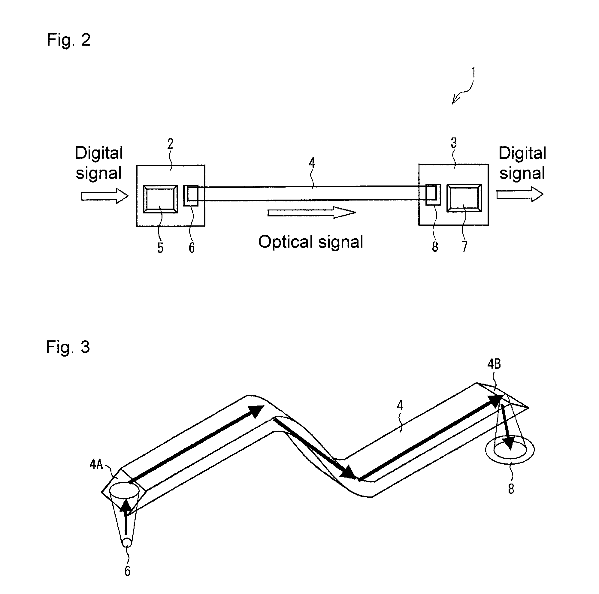
[0055]One embodiment of the present invention will be described with reference to FIG. 1 to FIG. 3. FIG. 2 shows a schematic configuration of an optical transmission module (communication module) according to the present embodiment. As shown in the figure, the optical transmission module 1 includes a light transmission processing section (transmission device) 2, a light reception processing section (reception device) 3, and an optical waveguide 4 serving as an optical transmission path.

[0056]The light transmission processing section 2 is configured to include a light emission drive unit 5 and a light emitting unit 6. The light emission drive unit 5 drives the light emission of the light emitting unit 6 based on an externally inputted digital signal. The light emission drive unit 5 is configured by a light emission drive IC (Integrated Circuit), and the like.

[0057]The light emitting unit 6 emits light based on drive control by the light emission drive unit 5. The light emitting unit ...

second embodiment

[0077]Another embodiment of the present invention will be described based on FIG. 4 to FIG. 7. FIG. 4 is a circuit diagram showing a schematic configuration of the amplification unit 7 of the light reception processing section 3 in the optical transmission module according to the present embodiment. The amplification unit 7 shown in FIG. 4 differs from the amplification unit 7 shown in FIG. 1 in that an amplification circuit 14 functioning as the LPF is arranged instead of the LPF 13, and the other configurations are the same. The same reference numerals are denoted for the configurations having similar functions as the configurations described in the above embodiment, and the description thereof will be omitted.

[0078]According to the above configuration, the LPF does not need to be added to the main path because the amplification circuit 14 functions as the LPF. Therefore, the circuit scale is prevented from increasing to reduce the noise from the digital circuit unit 20.

[0079]The ...

third embodiment

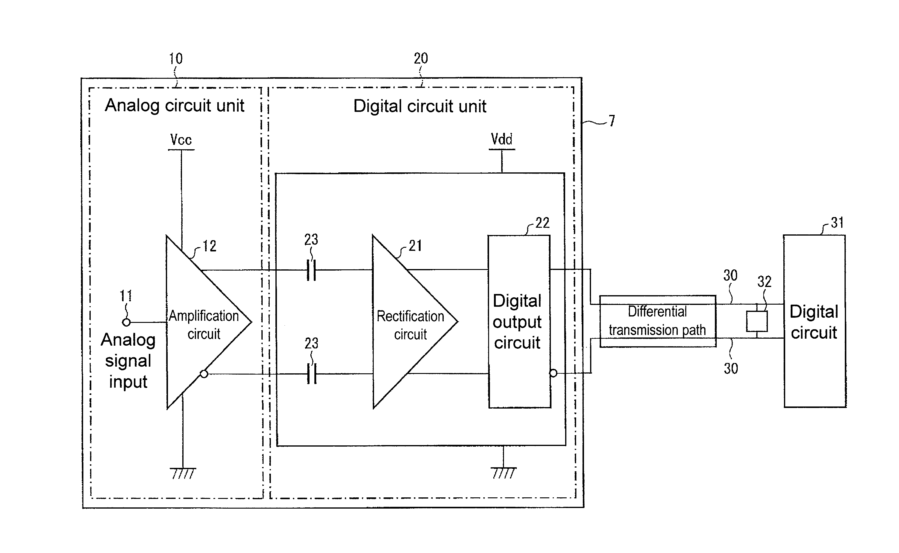
[0086]Still another embodiment of the present invention will now be described based on FIG. 8. FIG. 8 is a circuit diagram showing a schematic configuration of the amplification unit 7 in the light reception processing section 3 in the optical transmission module according to the present embodiment. The amplification unit 7 shown in FIG. 8 differs from the amplification unit 7 shown in FIG. 1 in that the LPF 13 is omitted because the amplification circuit 12 functions as the LPF and that capacitors 23, 23 are arranged on the main path between the amplification circuit 12 and the rectification circuit 21, and other configurations are the same. The same reference numerals are denoted for the configurations having the functions similar to the functions described in the above embodiment, and the description thereof will be omitted.

[0087]In the present embodiment, the amplification circuit 12 functions as the LPF, similar to the amplification circuit 14 shown in FIG. 4. The LPF thus does...


PUM


Abstract

It is possible to reduce a noise component mixed in an analog signal while suppressing increase of power consumption. An amplification unit amplifies the inputted analog signal and converts the amplified signal into a digital signal of a predetermined format for output. The amplification unit includes: an analog circuit unit for processing an analog signal; and a digital circuit unit for processing a digital signal; wherein the circuits are arranged on a substrate. The analog circuit unit includes: an amplification circuit for amplifying the inputted analog signal; and an LPF for cutting off a high frequency component of the amplified analog signal. The digital circuit unit includes: a rectification circuit which rectifies a waveform of the signal whose high-frequency component is cut off; and digital output circuit which converts the waveform-rectified signal into a digital signal of a predetermined format for output.

Description

BACKGROUND OF THE INVENTION[0001]1. Technical Field[0002]One or more embodiments of the present invention relate to a signal processing device and a signal processing method for amplifying an inputted analog signal, converting the amplified signal to a digital signal for output, as well as a reception device, a transmission / reception device, a communication module and an electronic device including the signal processing device. Specifically, one or more embodiments of the present invention relate to a signal processing device for processing signals received from a light waveguide through a light receiving element.[0003]2. Background Art[0004]In recent years, an optical transmission technique using an optical transmission path (light waveguide) such as an optical fiber is used for a data communication technique that enables large capacity data communication at high speed. In an optical transmission system using such an optical transmission technique, when a digital electric signal (h...

Claims


Application Information

Patent Timeline
Patent Type & Authority Patents(United States)
IPC IPC(8): H03M1/00H04B1/10H04B10/2507H04B10/40H04B10/43H04B10/50H04B10/60H04B10/69
CPCH03F3/087
Inventor ENAMI, AKIRAUNO, KEISUKEHOSOKAWA, HAYAMIHAMANA, KENTARONOSAKA, TETSUYA
Owner ORMON CORP
Why Eureka
Try Eureka