

Semiconductor memory component in cross-point architecture
a technology of memory components and semiconductors, applied in semiconductor devices, digital storage, instruments, etc., can solve the problems of increasing the surface area taken up by each memory cell, affecting the performance of the memory cell, so as to increase the conductivity of the memory cell
- Summary
- Abstract
- Description
- Claims
- Application Information
AI Technical Summary
Problems solved by technology
Method used
Image

Examples
Embodiment Construction
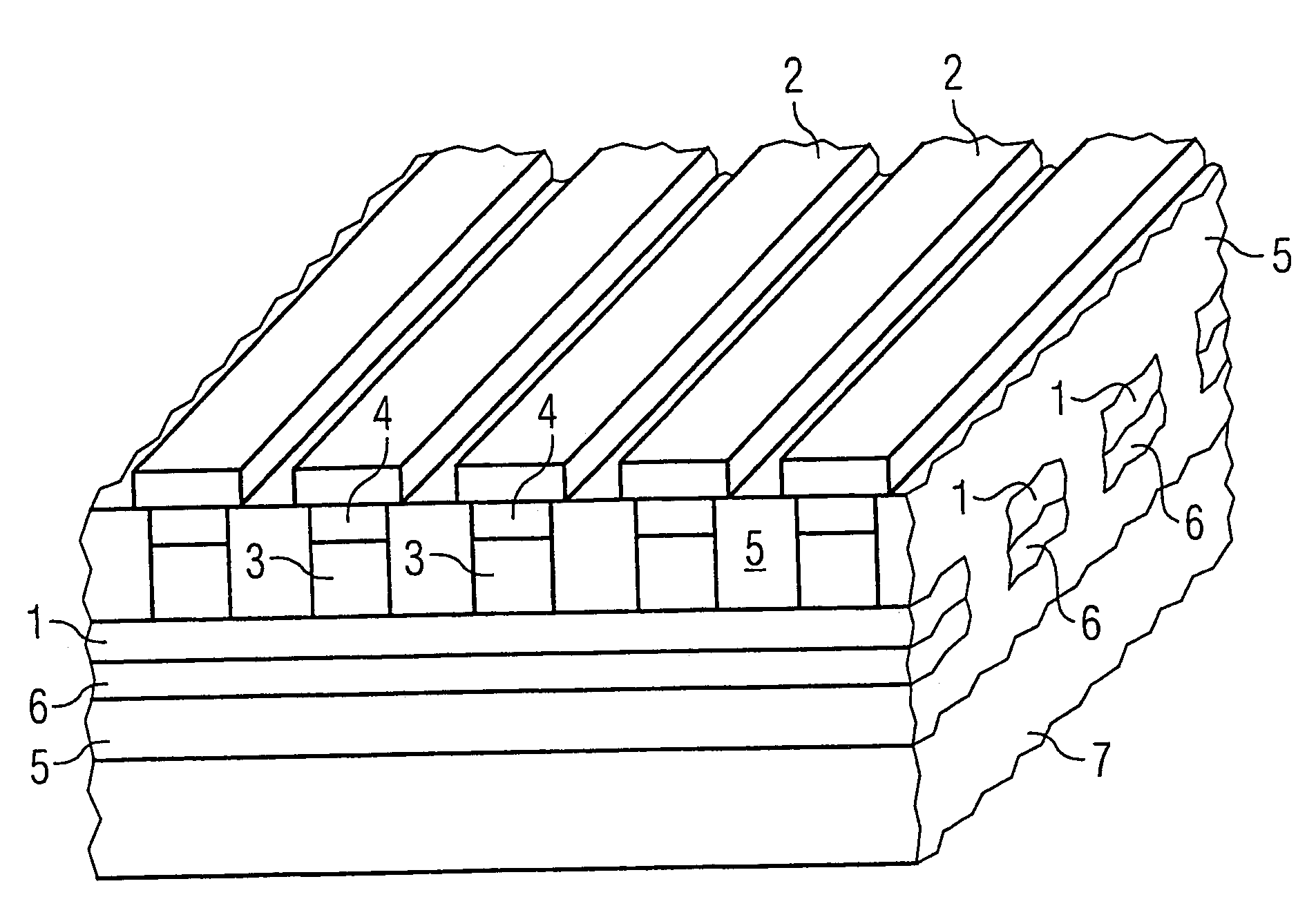
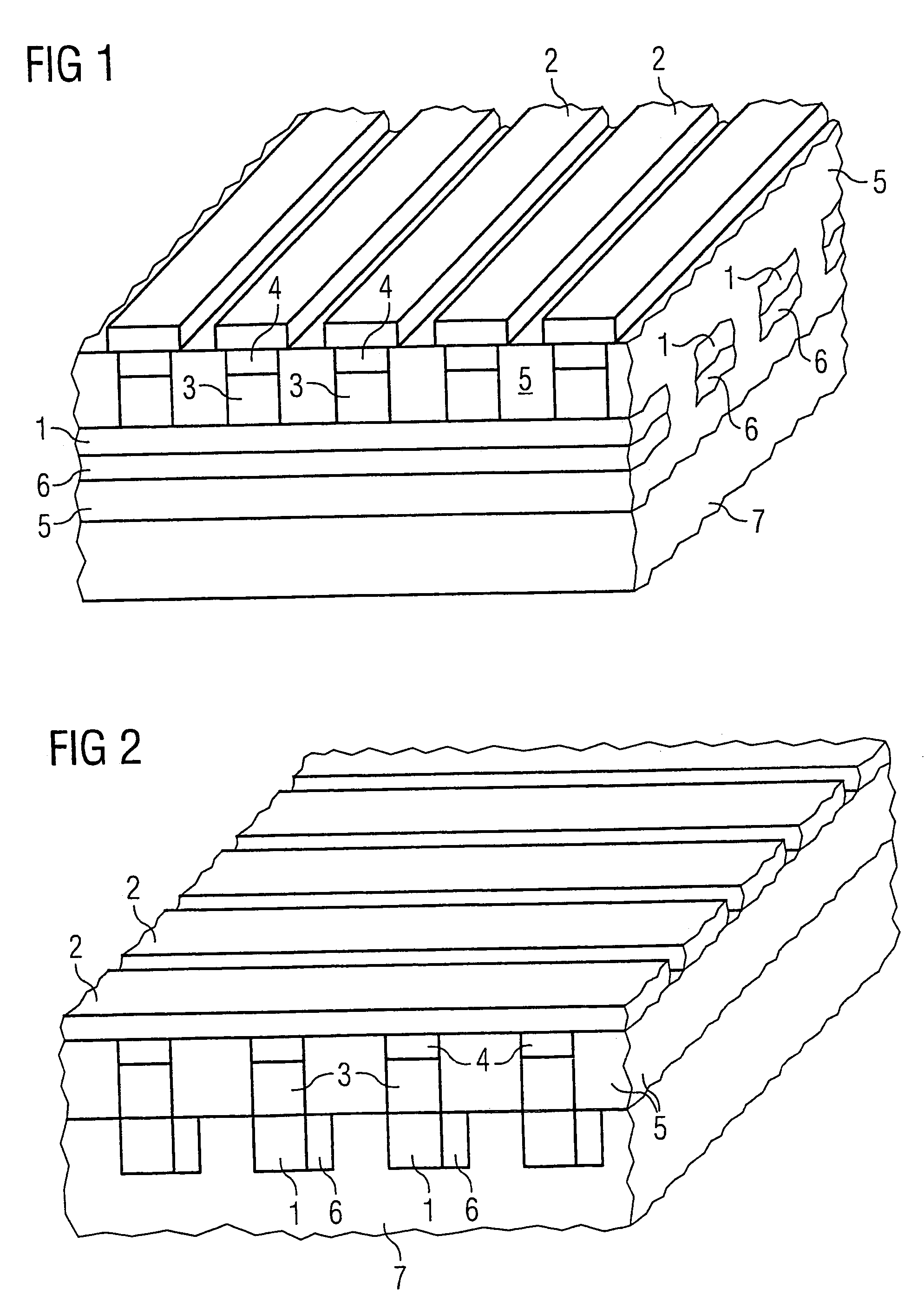
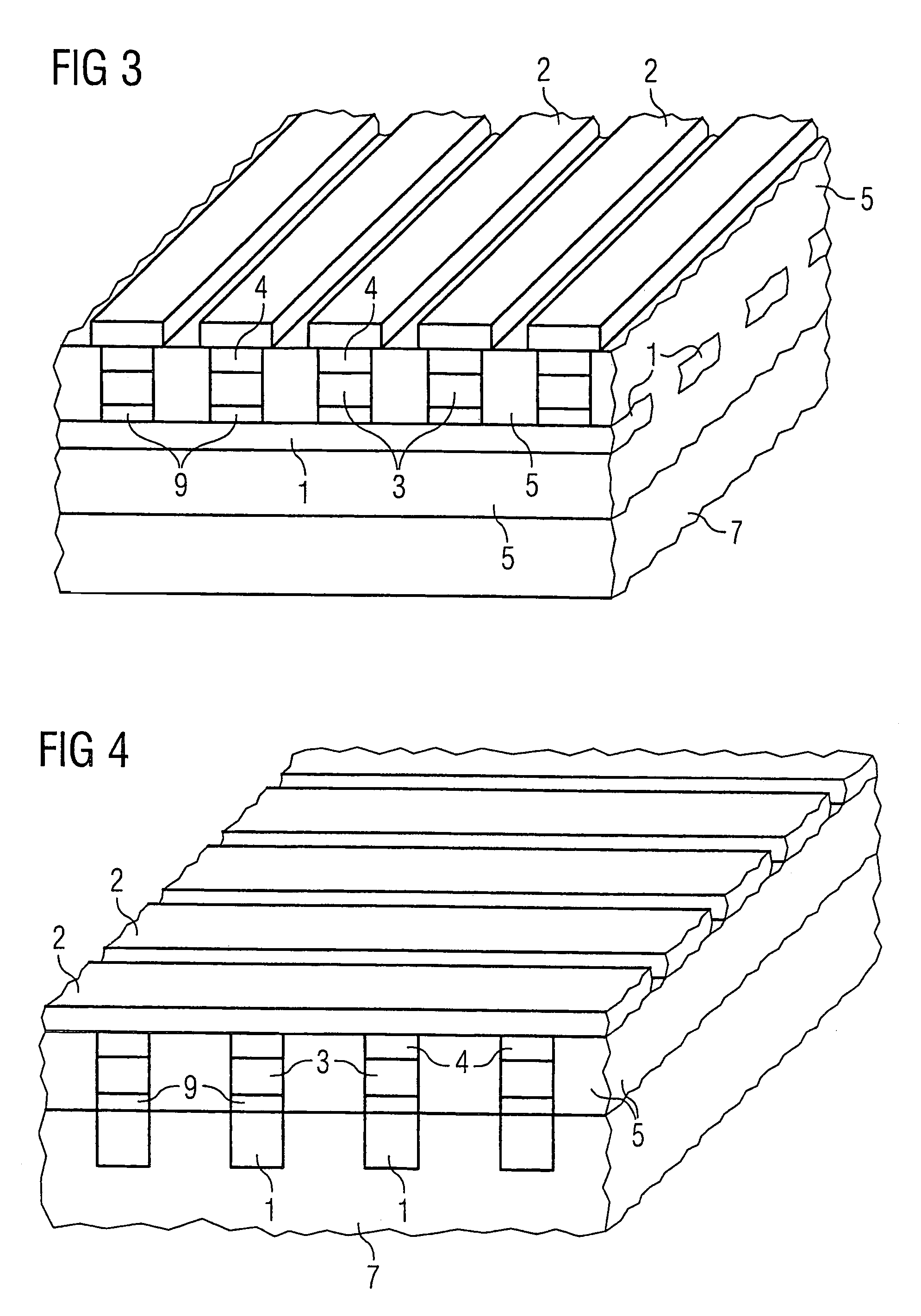
[0023]FIG. 1 illustrates a sectional view of a preferred configuration of a semiconductor memory component. The bit lines 1 are arranged parallel to and at a distance from one another below the memory cells, while the word lines 2 are arranged on the top side, running parallel to and at a distance from one another and transversely with respect to the bit lines. The word lines 2 may be a material that is used for interconnect structures, e.g., Al, Cu or W. At a respective crossing point of a corresponding bit line 1 and a word line 2 there is a programmable metalization memory cell, which comprises a storage region 3 and an electrode 4.
[0024]The storage region 3 contains a chalcogenide glass that, in combination with the topside electrode 4, forms a programmable metalization memory cell. The chalcogenide glass is undoped and therefore p-conducting at least adjacent to the bit line 1. The bit line is n-doped semiconductor material, e.g., n+-doped polysilicon, so that there is a pn jun...
PUM
 Abstract
Description
Claims
Application Information