Electro-optical element and method for manufacturing thereof, optical module and method for driving thereof
a technology of optical elements and electrooptical elements, applied in the direction of optical radiation measurement, instruments, semiconductor lasers, etc., can solve problems such as insufficient sensitivity
- Summary
- Abstract
- Description
- Claims
- Application Information
AI Technical Summary
Benefits of technology
Problems solved by technology
Method used
Image


Examples
first exemplary embodiment
1. Construction of an Electro-Optical Element
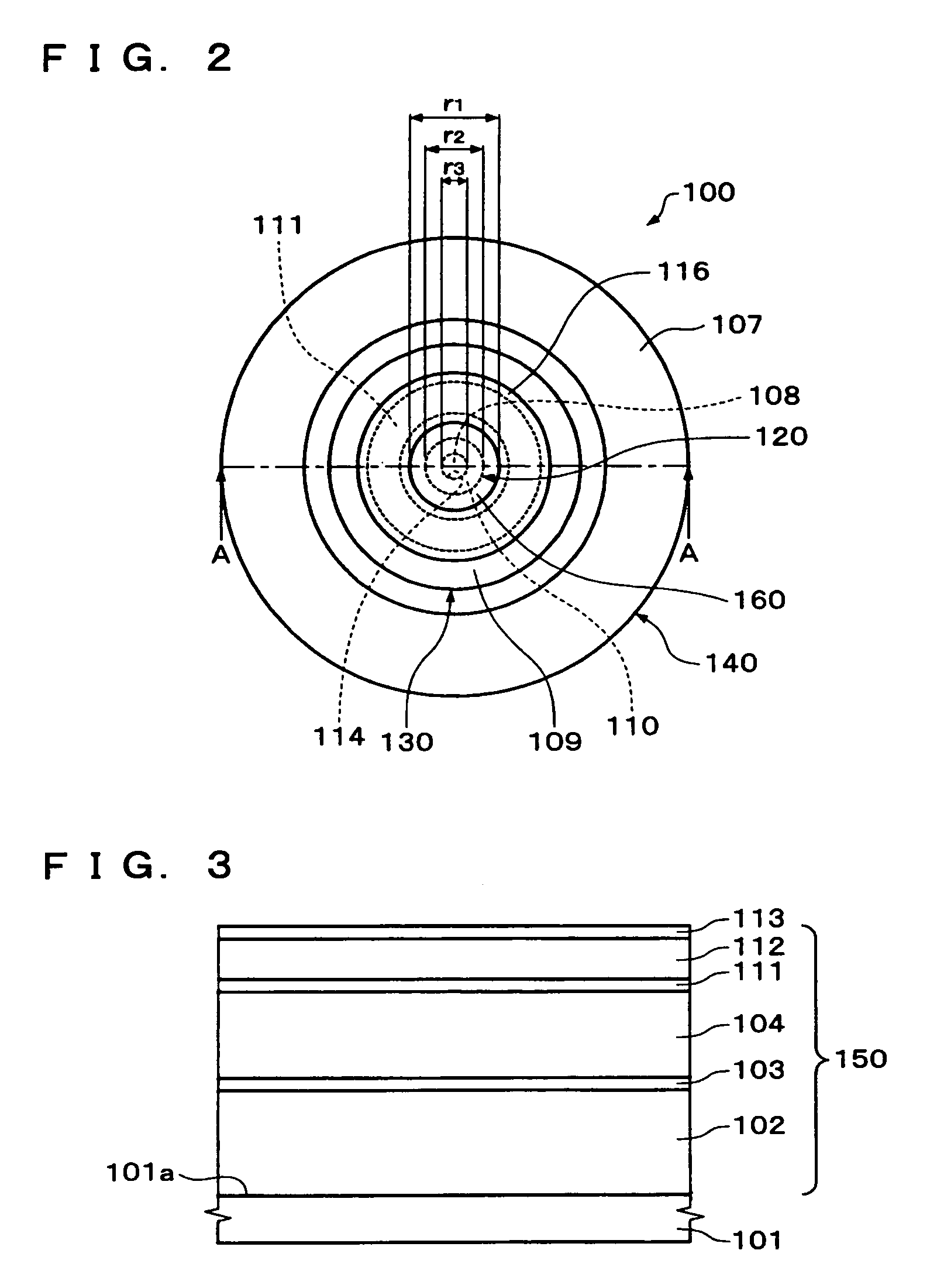
[0051]FIG. 1 is a schematic illustrating an electro-optical element 100 according to a first exemplary embodiment of the invention. FIG. 2 is a schematic illustrating the electro-optical element 100 in FIG. 1.
[0052]The electro-optical element 100 in the exemplary embodiment, as shown in FIG. 1, includes a light-emitting element part 140 and a light-receiving element part 120. In the exemplary embodiment, a case where the light-emitting element part 140 functions as a surface emitting semiconductor laser and the light-receiving element part 120 functions as a light-detecting part is described.
[0053]In this electro-optical element 100, a laser light can be emitted from an optical surface 108 in a direction that the light-emitting element part 140 and the light-receiving element part 120 are formed in layers. An optical member 160 is disposed at least on the optical surface 108. The light-emitting element part 140, the light-receiving elemen...
second exemplary embodiment
1. Construction of the Electro-Optical Element.
[0123]FIG. 11 is a schematic illustrating an electro-optical element 200 according to a second exemplary embodiment of the invention. In this exemplary embodiment, in the same manner as that of the first exemplary embodiment, a case where the light-emitting element part 240 functions as a surface emitting semiconductor laser and the light-receiving element part 220 functions as a light-detecting part is described.
[0124]The electro-optical element 200 of the exemplary embodiment differs from the electro-optical element 100 of the first exemplary embodiment in that the light-receiving element part 220 and the light-emitting element part 240 are deposited on a semiconductor substrate 201 in this order. As for the electro-optical element 200 of the exemplary embodiment, a similar construction element to a construction element described as “1XX” in the electro-optical element 100 of the first exemplary embodiment is described as “2XX”. There...
third exemplary embodiment
1. Construction of the Electro-Optical Element
[0135]FIG. 12 is a schematic illustrating an electro-optical element 300 according to a third exemplary embodiment of the invention. Also, FIG. 13 is a schematic illustrating the electro-optical element 300 shown in FIG. 12. In this exemplary embodiment, in the same manner as that of the first exemplary embodiment and the second exemplary embodiment, a case where the light-emitting element part 240 functions as a surface emitting semiconductor laser and the light-receiving element part 220 functions as a light-detecting part is described.
[0136]The electro-optical element 300 according to the exemplary embodiment includes the same construction as that of the electro-optical element 100 of the first exemplary embodiment. Therefore, a construction element that is substantively the same as that of the electro-optical element 100 of the first exemplary embodiment is labeled as the same, thereby omitting its detailed description.
[0137]In the e...
PUM
| Property | Measurement | Unit |
|---|---|---|
| wavelength | aaaaa | aaaaa |
| refractive index | aaaaa | aaaaa |
| wavelength λ | aaaaa | aaaaa |
Abstract
Description
Claims
Application Information
 - R&D
- Intellectual Property
- Life Sciences
- Materials
- Tech Scout
- Unparalleled Data Quality
- Higher Quality Content
- 60% Fewer Hallucinations
Browse by: Latest US Patents, China's latest patents, Technical Efficacy Thesaurus, Application Domain, Technology Topic, Popular Technical Reports.
© 2025 PatSnap. All rights reserved.Legal|Privacy policy|Modern Slavery Act Transparency Statement|Sitemap|About US| Contact US: help@patsnap.com