Optical transceiver module

a technology of optical transceiver and optical module, applied in the direction of dielectric characteristics, instruments, optical elements, etc., can solve the problems of limiting the density and speed of these optical modules, affecting the speed of these modules, and limiting the density of these modules. achieve the effect of improving the optical transceiver modul

Inactive Publication Date: 2009-05-26
IBM CORP
View PDF14 Cites 93 Cited by
  • Summary
  • Abstract
  • Description
  • Claims
  • Application Information

AI Technical Summary

Problems solved by technology

However, this current packaging approach limits both the density and the speed of these optical modules.
The density of these modules is limited because of the requirements for relatively large wire bond pads and because these modules are typically incorporated only on the perimeter of the chip.
Further, the speed of these modules is adversely impacted by electrical parasitics associated with the wire bond connections.
In addition, wire bonding makes packaging two-dimensional (2-D) arrays problematic by precluding the possibility of producing optical transmitters and receivers with a large number of parallel channels, such as, for example, greater than 24.
Moreover, GaAs and InP substrates, which are typically used as the starting material for producing photodiodes and VCSELs, are not transparent to a wavelength at substantially 850 nanometers (nm).

Method used


Image

  • Optical transceiver module
  • Optical transceiver module
  • Optical transceiver module

Examples


Embodiment Construction

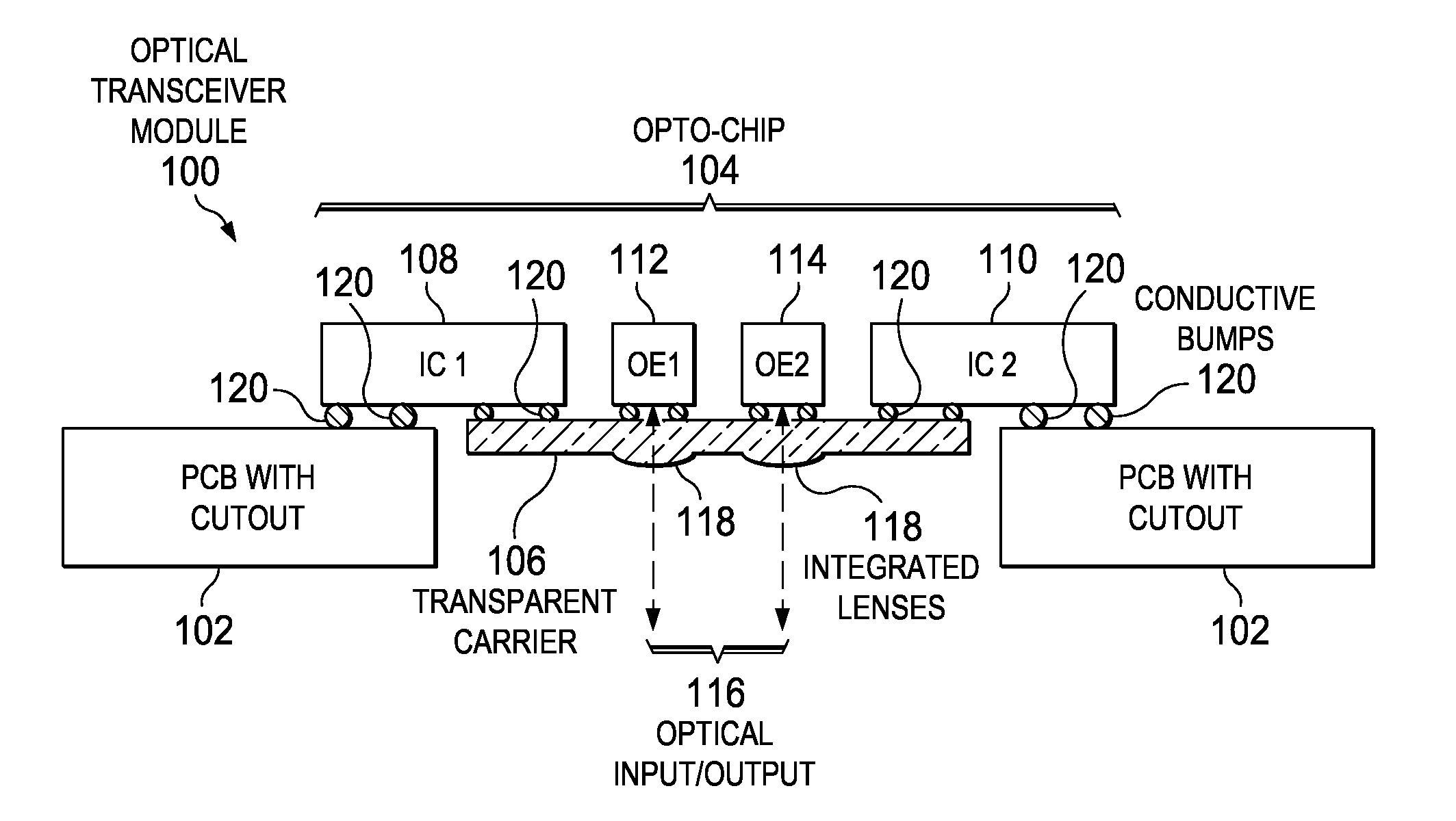
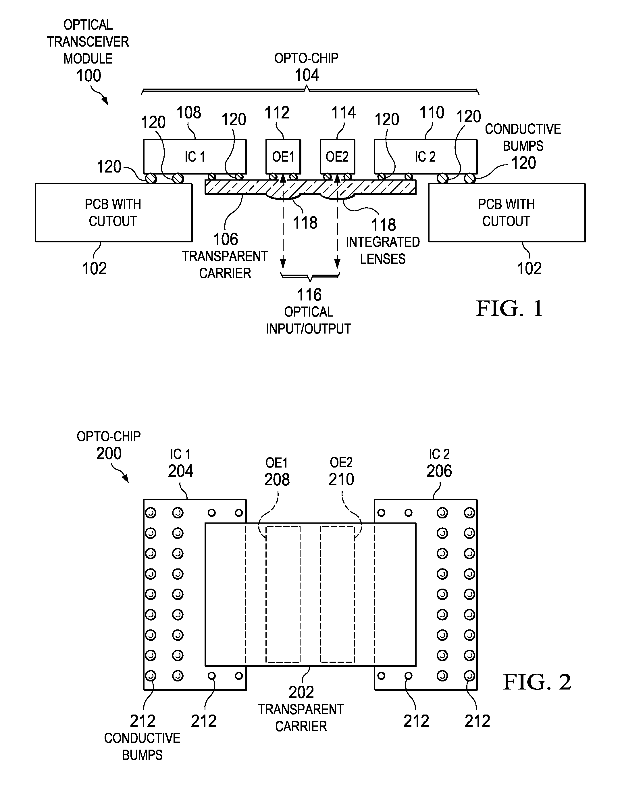
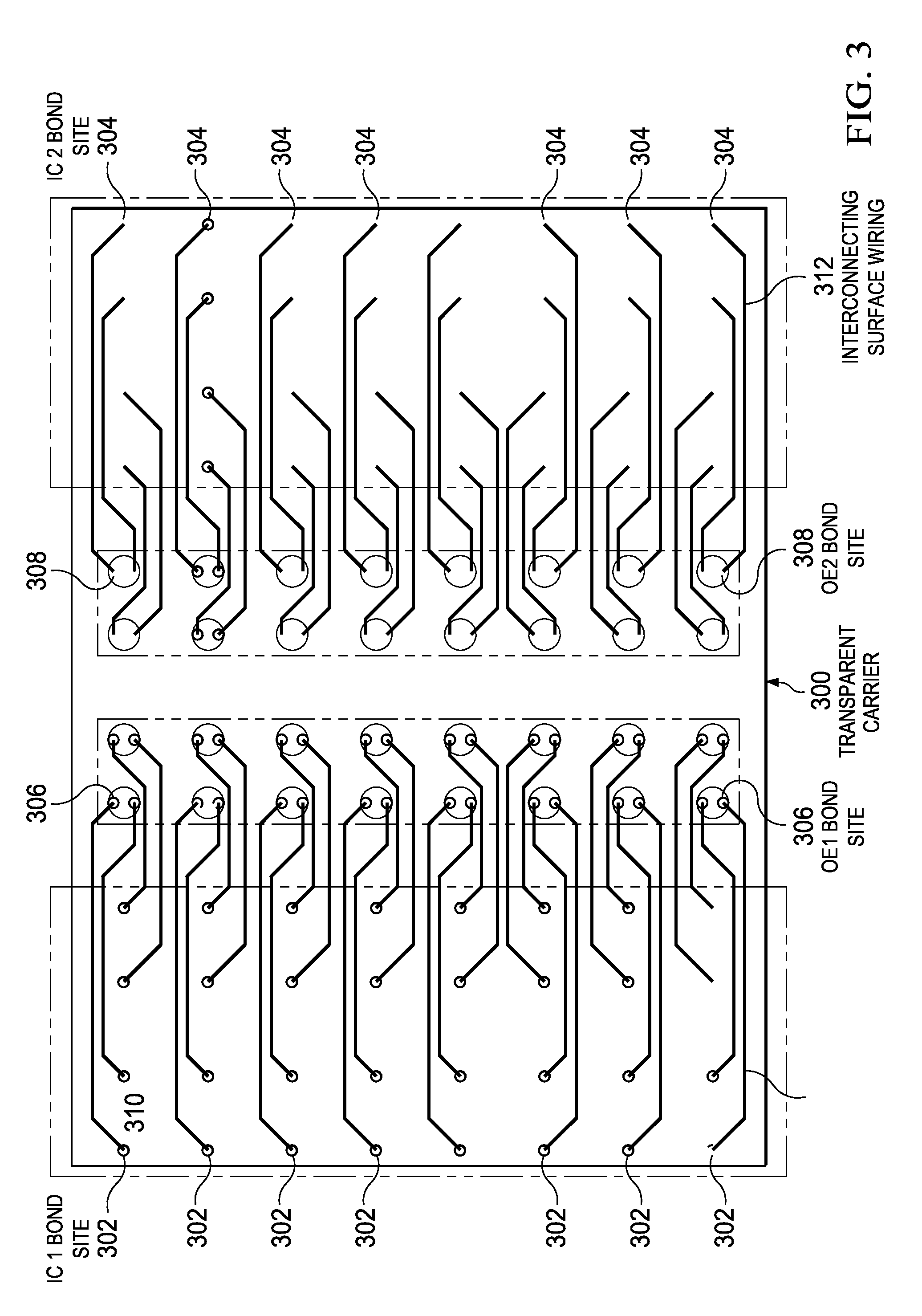
[0021]With reference now to the figures and in particular with reference to FIG. 1, an exemplary block diagram of an optical module apparatus is provided in which illustrative embodiments may be implemented. It should be appreciated that FIG. 1 is only exemplary and is not intended to assert or imply any limitation with regard to different illustrative embodiments. Many modifications to the depicted optical module may be made.

[0022]FIG. 1 depicts a block diagram of a side edge view of an optical transceiver module in which illustrative embodiments may be implemented. Optical transceiver module 100 is an electrical and optical component that is capable of transmitting and receiving pulses of light, which are used to communicate data. Optical transceiver module 100 includes printed circuit board (PCB) 102 and opto-chip 104.

[0023]PCB 102 mechanically supports and electronically connects electronic components, such as opto-chip 104, to other electronic components. PCB 102 may, for examp...


PUM


Abstract

An optical module. The optical module includes a printed circuit board and an opto-chip. The opto-chip includes a transparent carrier with an optoelectronic device array and an associated integrated circuit array that are flip chip attached to the transparent carrier. The optoelectronic device array and the associated integrated circuit array are interconnected via surface wiring with bond sites. In addition, the associated integrated circuit array extends beyond the transparent carrier to provide direct flip chip attachment of the opto-chip to the printed circuit board.

Description

[0001]This invention was made with Government support under Contract No.: MDA972-03-3-0004 awarded by Defense Advanced Research Projects Agency (DARPA). The Government has certain rights in this invention.BACKGROUND OF THE INVENTION[0002]1. Field of the Invention[0003]The present invention relates generally to an improved data processing system. More specifically, the present invention is directed to an optical transceiver module that utilizes a transparent carrier and one or more integrated circuits, which are attached to both the transparent carrier and a package.[0004]2. Description of the Related Art[0005]Today, separate 12-channel parallel optical transmitter and receiver modules are available that operate at up to five gigabits per second (Gb / s) per channel. These optical modules are based on one-dimensional (1×12) arrays of photodiodes and vertical cavity surface emitting lasers (VCSELs), which are typically manufactured on gallium arsenide (GaAs) or indium phosphoride (InP) ...

Claims


Application Information

Patent Timeline
Patent Type & Authority Patents(United States)
IPC IPC(8): G02B6/12G02B6/36
CPCG02B6/4201G02B6/4246H01L31/173H05K1/0274G02B6/4204H05K1/141H05K1/182H05K2201/0108H05K2201/09036H05K2201/10121G02B6/4245G02B6/4257G02B6/4259G02B6/426G02B6/428
Inventor BAKS, CHRISTIAN WILHELMUSDOANY, FUAD ELIASSCHOW, CLINT LEE
Owner IBM CORP
Why Eureka
Try Eureka