
Oriented self-location of microstructures with alignment structures

a technology of alignment structure and microstructure, applied in the assembly of microstructure devices, semiconductor devices, electrical equipment, etc., can solve the problems of limiting the number of different devices and material systems that can be successfully integrated, affecting the efficiency of growth and fabrication, and compromising growth and fabrication procedures optimized for a single device technology to accommodate dissimilar material systems. , to achieve the effect of facilitating the orientation of microstructures on the substra

Inactive Publication Date: 2007-05-29
HRL LAB
View PDF45 Cites 67 Cited by
  • Summary
  • Abstract
  • Description
  • Claims
  • Application Information

AI Technical Summary

Benefits of technology

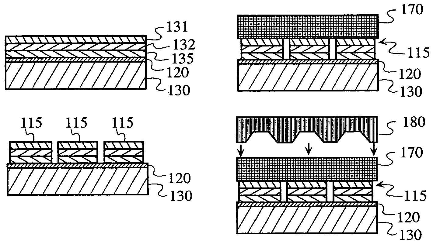
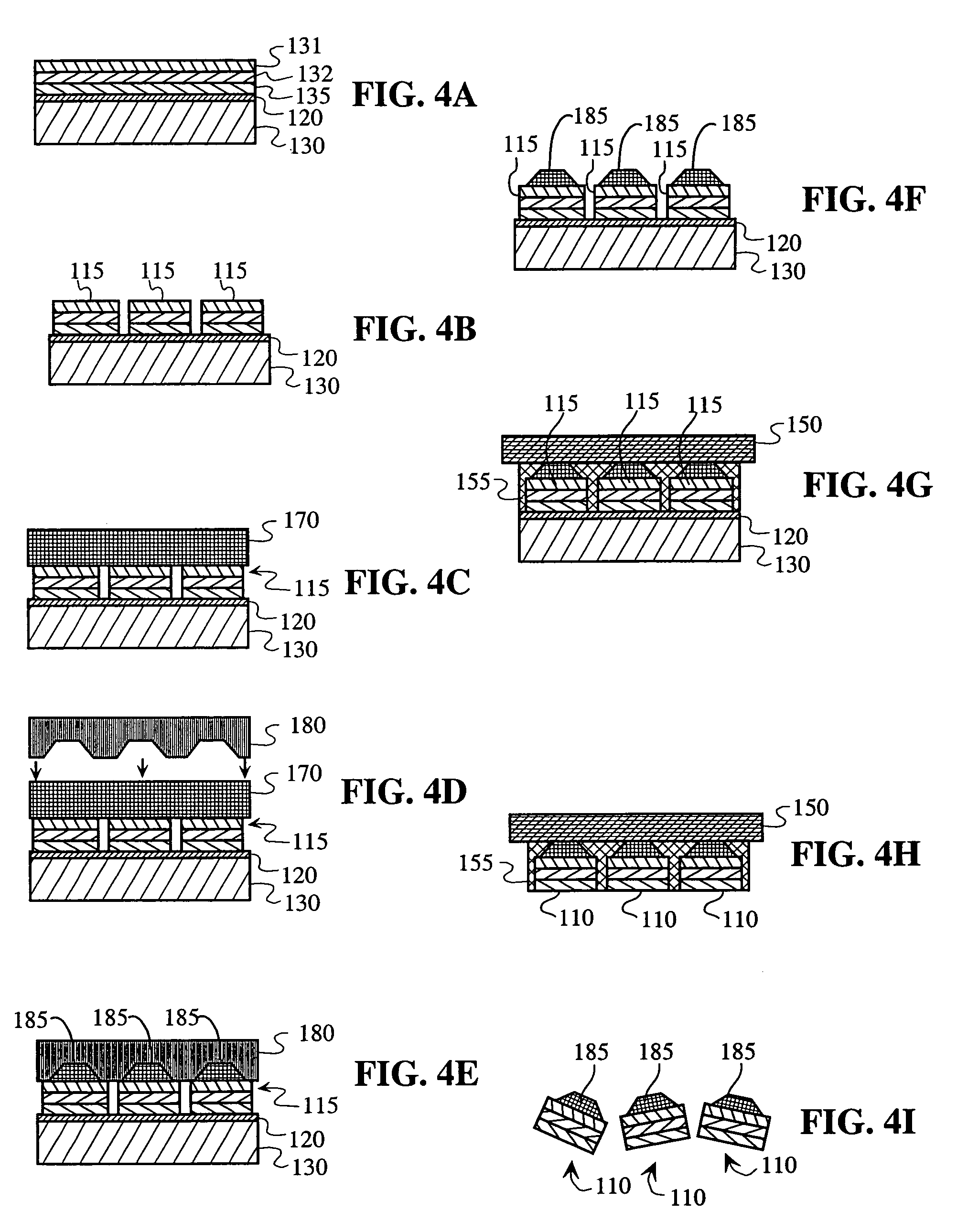
[0023]Embodiments of the present invention provide an electronic apparatus that comprises one or more microstructures positioned within a substrate in which the microstructures have a specific orientation. Embodiments of the present invention also provide a method for assembling microstructures on a substrate with a specific orientation. The orientation of the microstructures on the substrate is facilitated by the formation of alignment structures on the microstructures with contours that vary when the alignment structures are rotated 360° in a plane parallel to the substrate. The alignment structures are positioned within complementary-shaped receptacles in the substrate.

Problems solved by technology

Increasingly complex integrated electronic and optoelectronic systems require larger numbers of integrated circuits and devices to implement increasingly complex system functions.
Many complex integrated electronic and optoelectronic systems require the use of integrated circuits and devices that utilize different semiconductor technologies.
The heteroepitaxy approach may limit the number of different devices and material systems that can be successfully integrated.
Moreover, growth and fabrication procedures optimized for a single device technology often must be compromised to accommodate dissimilar material systems.
Finally, testing of individual portions of the integrated system may be made difficult by the fabrication techniques used to accommodate dissimilar material systems on a single wafer.
However, flip-chip is generally limited to relatively large size components, typically greater than 1 square millimeter, and is inefficient for the placement of large numbers of components due to its serial nature.
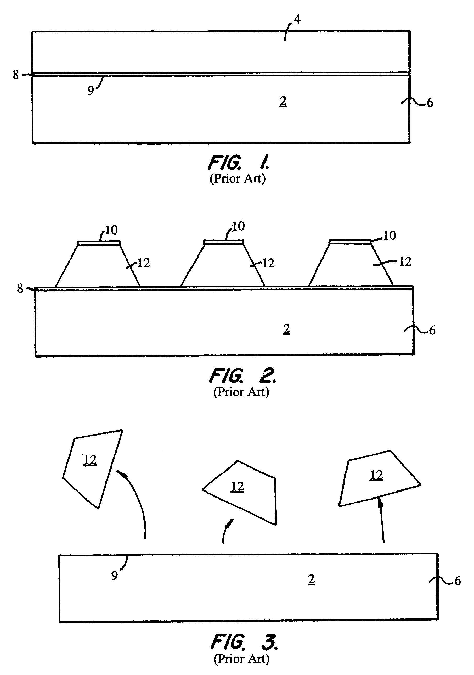
It is difficult to produce complementary shapes between receptacles and device microstructures using KOH etch techniques, because the microstructures require an exterior surface etch and the receptacles require an interior surface etch.
This leads to a loose fit.
These methods are typically limited to several microns of depth because the masking material and the polymer etch at the same rate.
Variations in the orientations of the microstructures positioned within the receptacles complicates the steps needed to make electrical, optical, or other types of connections to the microstructures.
The variations in the orientations may also limit or complicate the electrical or optical designs implemented by the microstructures.
The three-dimensional shapes of the shaped blocks comprising the microstructures or portions thereof and the complementarily shaped receptacles may also hinder the self-alignment capabilities of the microstructures.
Due to these shapes, a microstructure may be introduced in a skewed fashion to the corresponding receptacle, causing the microstructure to become stuck in the receptacle, but not properly seated in the receptacle.

Method used


Image

  • Oriented self-location of microstructures with alignment structures
  • Oriented self-location of microstructures with alignment structures
  • Oriented self-location of microstructures with alignment structures

Examples


Embodiment Construction

[0043]The present invention will now be described more fully hereinafter with reference to the accompanying drawings, in which preferred embodiments of the invention are shown. This invention may be embodied in many different forms and should not be construed as limited to the embodiments set forth herein. Further, the dimensions of layers and other elements shown in the accompanying drawings may be exaggerated to more clearly show details. The present invention should not be construed as being limited to the dimensional relations shown in the drawings, nor should the individual elements shown in the drawings be construed to be limited to the dimensions shown.

[0044]According to an embodiment of the present invention, a method for assembling device and integrated circuit components on a substrate with a specific orientation using fluid-based transport or other mass dispersing techniques is provided. Specific orientations are accomplished by using uniquely shaped alignment structures ...


PUM


Abstract

An electronic apparatus comprising one or more microstructures on a substrate and a method for fabricating the electronic apparatus. The microstructures have alignment structures that allow the microstructures to be oriented in receptacles having shapes that are complementary to the shapes of the alignment structures. The alignment structures are shapes that vary when rotated 360°, such that the microstructures are positioned at a specific orientation in the receptacles.

Description

CROSS-REFERENCE TO RELATED APPLICATIONS[0001]The present application is related to and claims benefit under 35 U.S.C. 119(e) to copending U.S. Provisional Application No. 60 / 490,193, titled “Oriented Self-Location of Microstructures with Alignment Structures,” filed Jul. 25, 2003. The contents of U.S. Provisional Application No. 60 / 490,193 are incorporated herein by reference in their entirety.[0002]The present disclosure is related to the following copending and commonly assigned United States patent applications, all of which are incorporated herein by reference in their entireties: “Method For Assembly of Complementary-Shaped Receptacle Site and Device Microstructures,” U.S. patent application Ser. No. 10 / 218,052, filed Aug. 12, 2002; “Process for Producing High Performance Interconnects,” U.S. patent application Ser. No. 10 / 256,334, filed Sep. 26, 2002; and “Process For Assembling Three-Dimensional Systems On A Chip And Structure Thus Obtained,” U.S. patent application Ser. No. ...

Claims


Application Information

Patent Timeline
Patent Type & Authority Patents(United States)
IPC IPC(8): H01L21/00
CPCB81C3/002H01L21/6835H01L24/95H01L25/50B81C2203/058H01L25/0657H01L29/0657H01L2221/68363H01L2224/95085H01L2924/01013H01L2924/01078H01L2924/01079H01L2924/09701H01L2924/10329H01L2924/14H01L2924/01005H01L2924/01006H01L2924/01019H01L2924/01033H01L2924/15787H01L2224/95136H01L2924/00
Inventor BREWER, PETER D.
Owner HRL LAB
Learn More