Connecting structure of circuit board and method for manufacturing the same

a technology of connecting structure and circuit board, which is applied in the direction of fixed connections, dielectric characteristics, thermoplastic polymer dielectrics, etc., can solve the problems of large pressing power required for collapsing, difficult to reduce increase the etc., to achieve the effect of reducing the electrical connection resistance of the contact portion, high precision and easy adjustment of positions

Inactive Publication Date: 2007-06-12
PANASONIC CORP
View PDF7 Cites 58 Cited by
  • Summary
  • Abstract
  • Description
  • Claims
  • Application Information

AI Technical Summary

Benefits of technology

[0014]According to this configuration, in the contact portion between the first conductor pattern and the second conductor pattern, an insulating material such as an adhesive is not included, both conductors are brought into direct contact with each other over the entire surface of the contact portion. Therefore, the connection resistance of the contact portion can be reduced. Furthermore, since solder, conductive adhesive, or the like, is not used in connection, it is possible to prevent defects such as short circuiting caused by solder, conductive adhesive, or the like, flowing to neighboring conductor patterns at the time of connection. As a result, a connecting structure of a circuit board having a small connection resistance even when conductor patterns are arranged with a fine pitch can be manufactured in an improved yield.
[0027]As mentioned above, in the connecting structure of the circuit board of the present invention, since an insulating material such as an adhesive is not included in a contact portion between the first conductor patterns and the second conductor patterns, the conductors can be brought into direct contact with each other over the entire surface of the contact portion. Therefore, the electrical connection resistance of the contact portion can be reduced. Furthermore, since solder, conductive adhesive, or the like, is not used in connection, it is possible to prevent defectives such as short circuit caused by solder, conductive adhesive, or the like, flowing to neighboring conductor patterns at the time of connection. As a result, a connecting structure having a small electric connection resistance even when conductor patterns are arranged with a fine pitch can be manufactured in an improved yield.

Problems solved by technology

Therefore, it is difficult to reduce connection resistance of a contact portion.
In particular, when pattern pitches of first conductor patterns 504 and second conductor patterns 510 are small and the contact area is small, such a displacement or remaining adhesive resin 512 may easily cause defects including short circuit between neighboring conductor patterns and an increase in the connection resistance of the contact portion.
In the case of such a material, a large pressing power is required for collapsing and expanding the material.
Furthermore, even when such a large pressure power is applied, when fine convex and concave portions exist in the electrode portion, it is difficult to completely remove all the liquid electrically insulating adhesive existing in the concave portion.
Therefore, this electrically insulating adhesive may remain in a part of the electrode surface, making it difficult to satisfactorily reduce the connection resistance of the contact portion.

Method used


Image

  • Connecting structure of circuit board and method for manufacturing the same
  • Connecting structure of circuit board and method for manufacturing the same
  • Connecting structure of circuit board and method for manufacturing the same

Examples


first embodiment

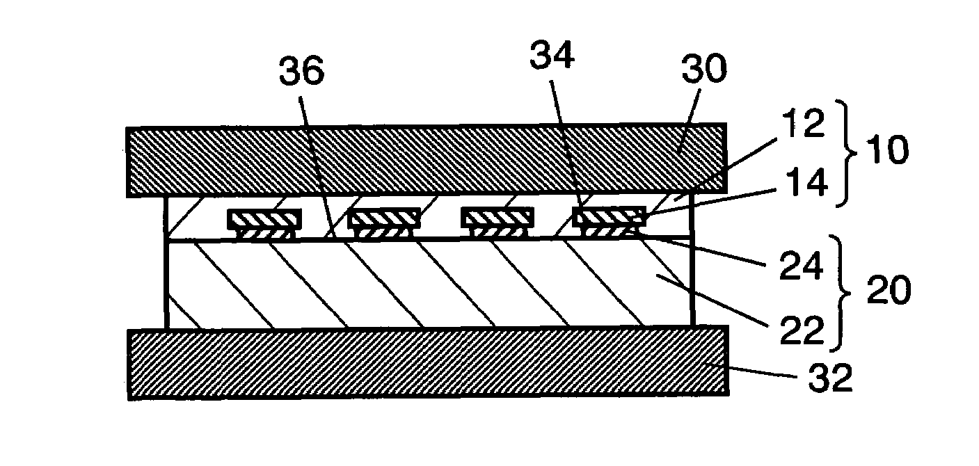
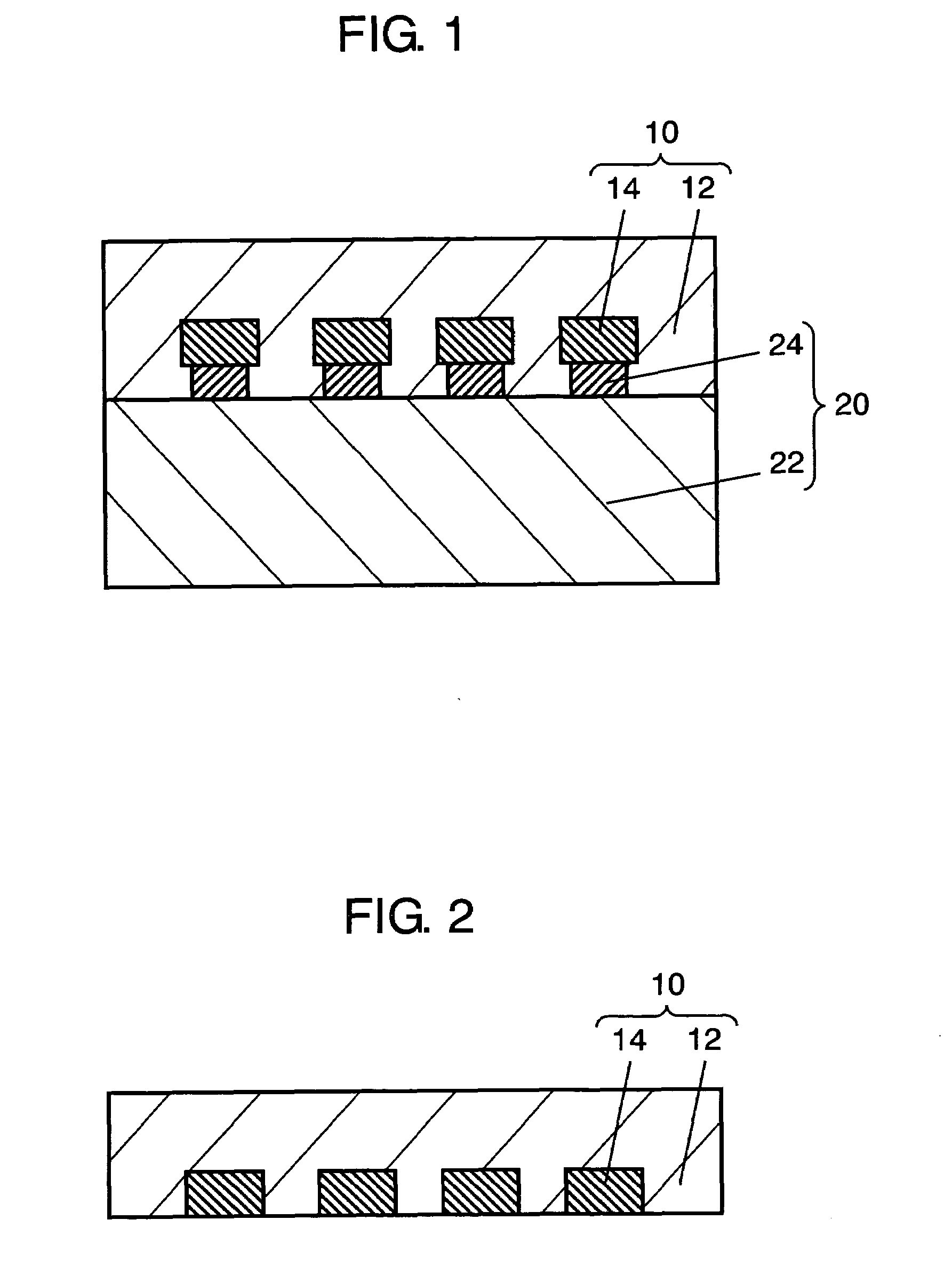
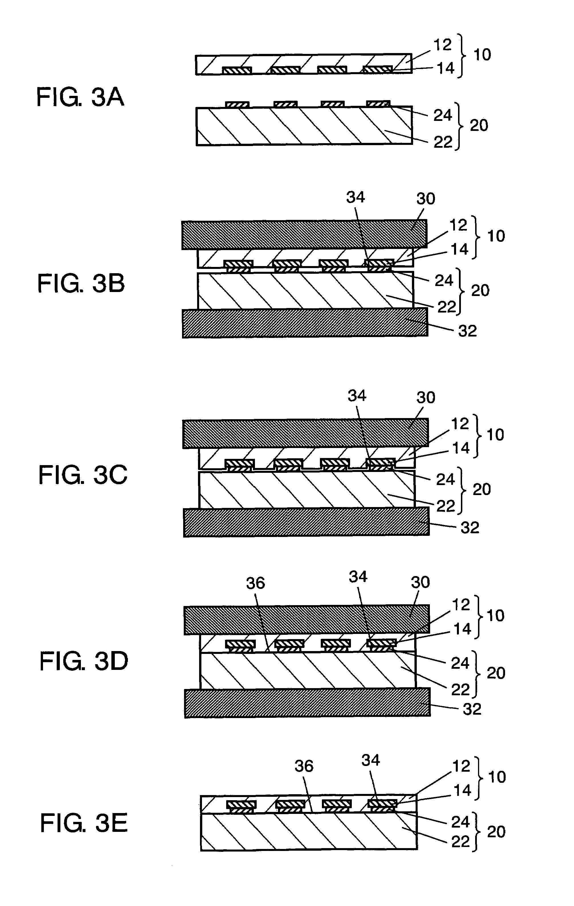
[0037]FIG. 1 is a sectional view of a main part of a connection portion showing a connecting structure of a circuit board according to a first embodiment of the present invention. In the configuration of the connecting structure of the circuit board of this embodiment, first circuit board 10 and second circuit board 20 are electrically connected to each other via first conductor patterns 14 and second conductor patterns 24, and first resin base material 12 of first circuit board 10 and second resin base material 22 of second circuit board 20 are bonded to each other. This bonding is carried out by thermal fusing of resin base material 12, when a material having a thermoplastic property and a thermal fusing property is used for first resin base material 12 of first circuit board 10.

[0038]FIG. 2 is a sectional view of a connection portion of first circuit board 10 shown in FIG. 1. In first circuit board 10, first conductor patterns 14, which are connection portions, are formed so that...

second embodiment

[0072]FIGS. 6A and 6B are sectional views showing main steps of a method for manufacturing a connecting structure of a circuit board according to a second embodiment of the present invention. FIG. 6A is a sectional view showing first circuit board 40. FIG. 6B is a sectional view showing a state in which first circuit board 40 and second circuit board 20 are pressed until first conductor patterns 44 and second conductor patterns 24 are brought into contact with each other. Note here that an upper heating pressing plate and a lower heating pressing plate for pressing are not shown.

[0073]The connecting structure of the circuit board of this embodiment is different from that of the first embodiment in the structures of first conductor patterns 44 of first circuit board 40. That is to say, in this embodiment, first conductor patterns 44 of first circuit board 40 are embedded in first resin base material 42, and surface 48 of first conductor pattern is disposed inwardly from the surface l...

third embodiment

[0084]FIGS. 7A and 7B are sectional views showing main steps of a method for manufacturing a connecting structure of a circuit board according to a third embodiment of the present invention.

[0085]FIG. 7A is a sectional view showing first circuit board 52. FIG. 7B is a sectional view showing a state in which first circuit board 52 and second circuit board 20 are pressed until first conductor patterns 56 and second conductor patterns 24 are brought into contact with each other. Note here that an upper heating pressing plate and a lower heating pressing plate for pressing are not shown.

[0086]The connecting structure of the circuit board of this embodiment is different from that of the first embodiment in the structure of first conductor patterns 56 of first circuit board 52. In this embodiment, as shown in FIG. 7A, first conductor patterns 56 of first circuit board 52 are formed on the surface of first resin base material 54 and are not embedded in first resin base material 54. Therefo...


PUM

PropertyMeasurementUnit
temperatureaaaaaaaaaa
softening temperatureaaaaaaaaaa

Abstract

First circuit board 10 including first resin base material 12 which is softened by heating and has a fusing property, and a plurality of first conductor patterns 14 formed on a surface of first resin base material 12, and second circuit board 20 on which a plurality of second conductor patterns 24 are formed with the same pitch as that of first conductor patterns 14 are provided. In the configuration, first conductor patterns 14 and second conductor patterns 24 are brought into mechanical contact with each other to provide electrical conduction; first resin base material 12 covers first conductor patterns 14 and second conductor patterns 24 and is bonded to second resin base material 22 of second circuit board 20, thereby connecting first circuit board 10 and second circuit board 20 to each other.

Description

BACKGROUND OF THE INVENTION[0001]1. Field of the Invention[0002]The present invention relates to a connecting structure for connecting between circuit boards. More specifically, the present invention relates to a connecting structure for connecting conductor patterns to each other by bringing them into contact with each other and a method for manufacturing the connecting structure.[0003]2. Background Art[0004]FIGS. 8A to 8C are sectional views showing a connection portion for illustrating main steps of a method for connecting conductor patterns to each other in a conventional circuit board. In FIG. 8A, first circuit board 500 includes first resin base material 502 and convex first conductor patterns 504 formed on the surface of first resin base material 502. Furthermore, second circuit board 506 includes second resin base material 508 and convex second conductor patterns 510 formed on the surface of second resin base material 508. First conductor patterns 504 of first circuit board ...

Claims


Application Information

Patent Timeline
Patent Type & Authority Patents(United States)
IPC IPC(8): H01R12/00
CPCH01R43/0207H05K3/361H01R12/52H05K3/107H05K2201/0129H05K2201/0376H05K2201/10977H05K2203/0278H05K2203/065
Inventor SAKURAI, DAISUKENISHIKAWA, KAZUHIROTSUKAHARA, NORIHITO
Owner PANASONIC CORP
Why Eureka
Try Eureka