Semiconductor memory and system apparatus
a technology of system apparatus and memory, applied in the field of semiconductor memory and system apparatus, can solve the problems of reset internal circuit and increase the chance of failure, and achieve the effect of reducing the wiring area of a signal line of the reset signal, reducing the chance of failure, and reliability initializing the internal circui
- Summary
- Abstract
- Description
- Claims
- Application Information
AI Technical Summary
Benefits of technology
Problems solved by technology
Method used
Image
Examples
first embodiment
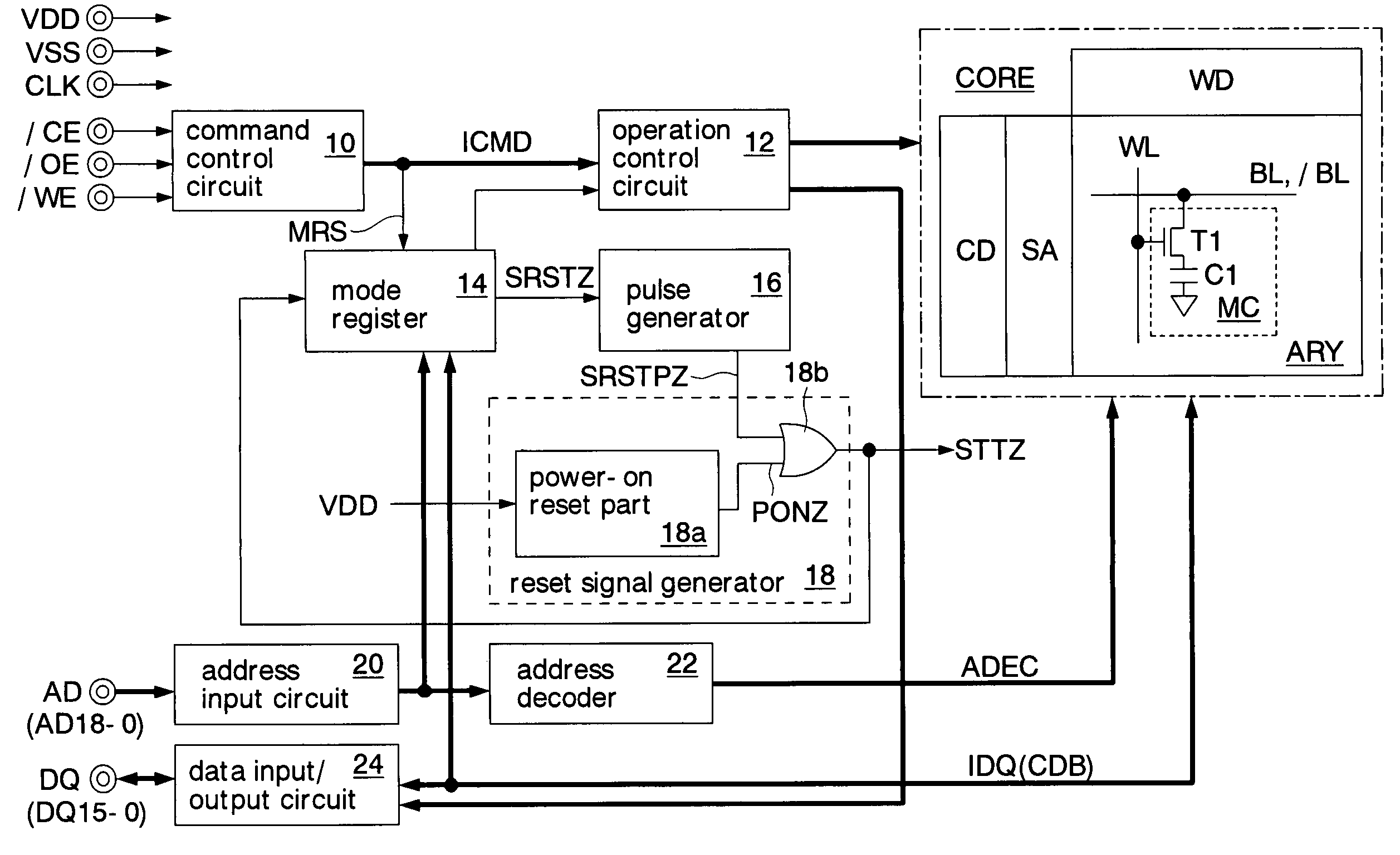
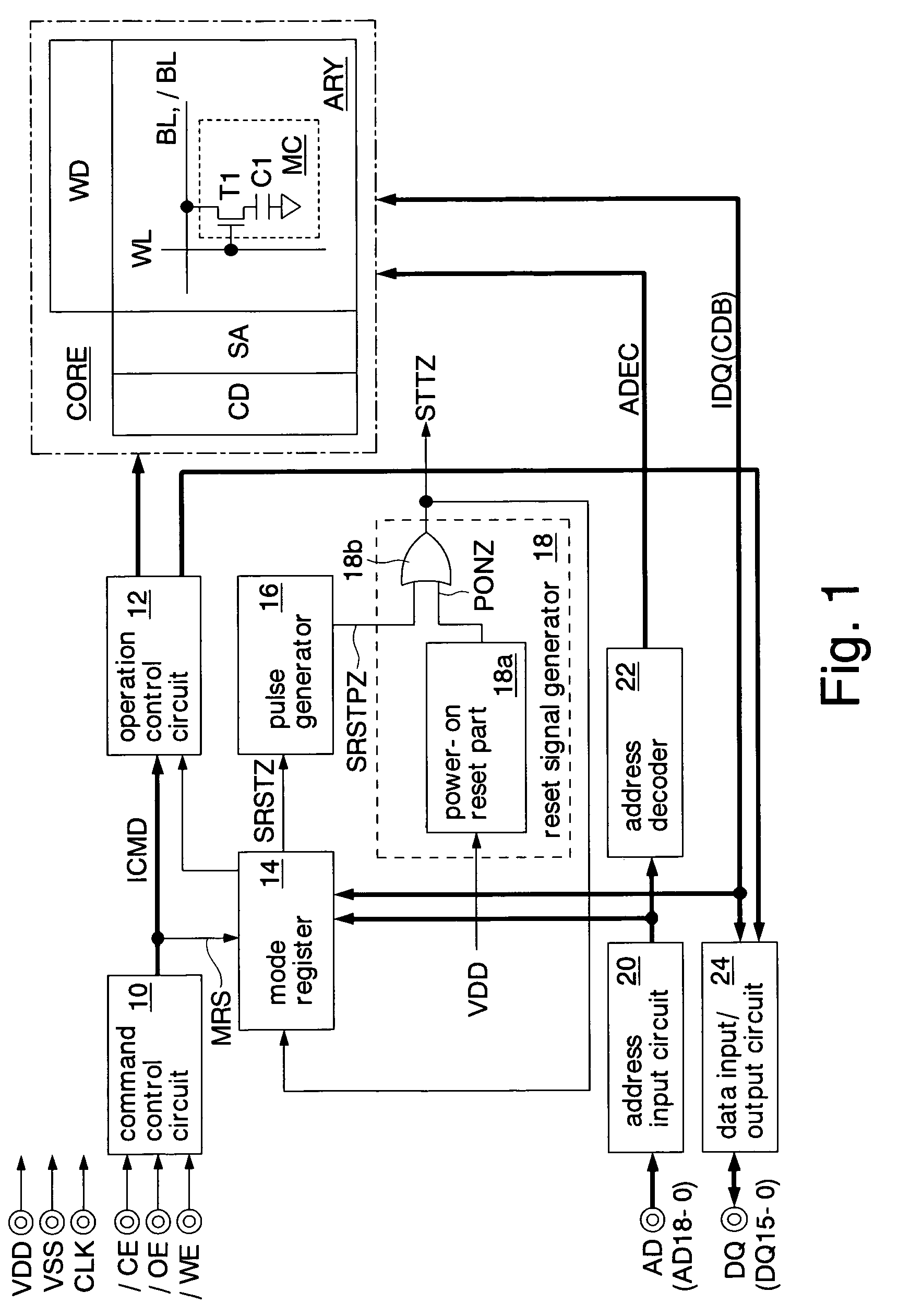
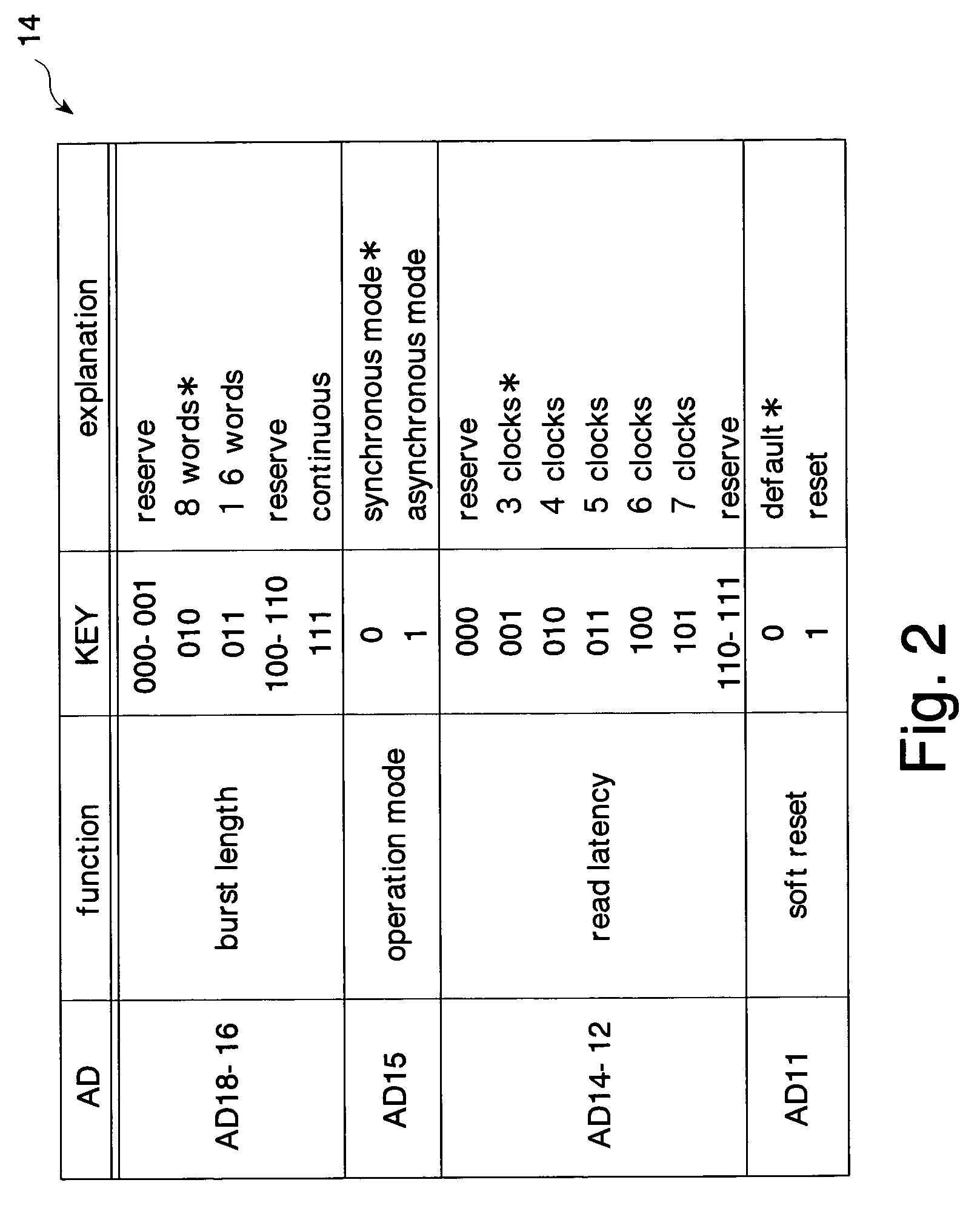
[0028]FIG. 1 illustrates a semiconductor memory according to the present invention. The semiconductor memory is formed as, for example, a fast cycle RAM (FCRAM) using a CMOS process technology. The FCRAM, which has a memory core of a DRAM, is a type of pseudo SRAM having an SRAM interface. The FCRAM has operation modes including a synchronous operation mode that performs a burst operation in synchronization with an external clock CLK, in addition to an asynchronous operation mode such as the SRAM that operates asynchronous to a clock. The FCRAM includes a command control circuit 10, an operation control circuit 12, a mode register 14, a pulse generator 16, a reset signal generator 18, an address input circuit 20, an address decoder 22, a data input / output circuit 24, and a memory core CORE.
[0029]The command control circuit 10 receives a chip enable signal / CE, an output enable signal / OE, and a write enable signal / WE, as external commands, decodes the received external commands, an...
third embodiment
[0060]In the above-mentioned third embodiment, an example where the soft reset pulse signal SRSTPZ is output from the reset output terminal has been described. However, the present invention is not limited thereto. For example, the reset signal STTZ may be output from the reset output terminal.
[0061]In the first and second embodiments, examples where each bit of the register part of the mode registers 14 and 14A is set by the external address signal AD have been described. However, the present invention is not limited thereto. For example, the same advantages can be obtained with the external data signal DQ constructed with a number of bits, such as the external address signal AB.
[0062]Moreover, the mode register 14A (FIG. 6) of the second embodiment can be applied to the FCRAM of the first embodiment. Also, the mode register 14 (FIG. 2) of the first embodiment can be applied to the FCRAM of the second embodiment. In addition, The FCRAM of the second embodiment can be applied to the...
PUM
 Abstract
Description
Claims
Application Information


