Flat panel display with thin film transistor (TFT)

Active Publication Date: 2007-09-04
SAMSUNG DISPLAY CO LTD
View PDF12 Cites 7 Cited by
  • Summary
  • Abstract
  • Description
  • Claims
  • Application Information

AI Technical Summary

Benefits of technology

[0017]The invention provides a flat panel display which can adjust a white balance to a proper level wit

Problems solved by technology

Thin film transistors using amorphous silicon can be deposited at a low temperature, but have degraded electrical characteristics and low reliability, and as such, are generally not suitable for large-sized display devices.
Accordingly, achieving a proper color

Method used


Image

  • Flat panel display with thin film transistor (TFT)
  • Flat panel display with thin film transistor (TFT)
  • Flat panel display with thin film transistor (TFT)

Examples


Embodiment Construction

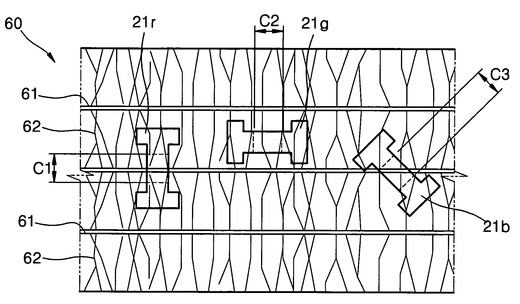
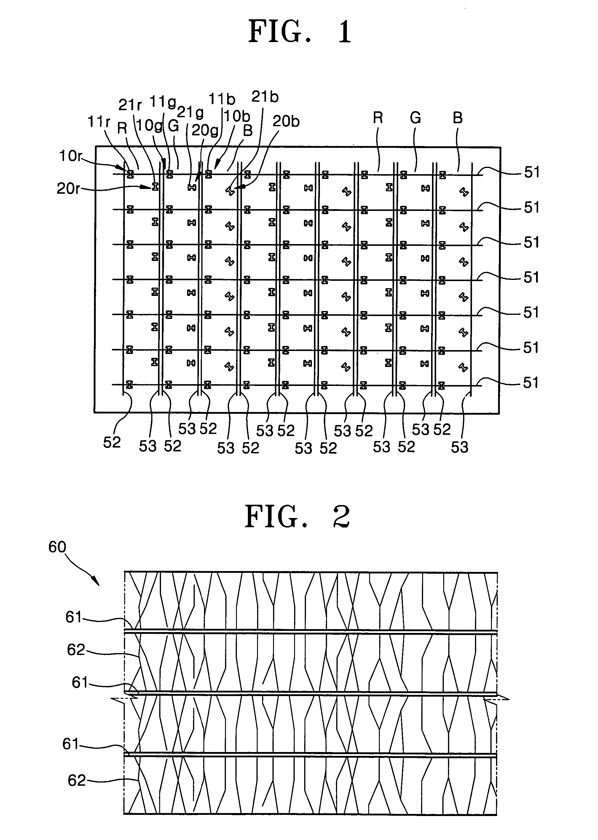
[0061]FIG. 1 is a plan view of a structure of a TFT active layer of an AM-type organic EL display according to an exemplary embodiment of the present invention. Referring to FIG. 1, the organic EL display includes a plurality of pixels, each of which is formed by repetitively arranging of a group of R, G, and B sub-pixels in a vertical direction. However, the present invention is not limited to the above sub-pixel arrangement. For example, sub-pixels of different colors can be arranged in various patterns, such as, a mosaic pattern or a lattice pattern to form a pixel.

[0062]In the organic EL display of FIG. 1, a plurality of gate lines 51 are arranged horizontally, and a plurality of data lines 52 are arranged vertically. Driving lines 53 for supplying power are also arranged vertically. One sub-pixel is defined by one gate line 51, one data line 52, and one driving line 53.

[0063]Each of the sub-pixels includes at least two TFTs, that is, a first TFT and a second TFT. First TFTs 10r...


PUM


Abstract

A flat panel display which can adjust a white balance to a proper level without changing the sizes of driving TFT active layers, even when an identical driving voltage is applied. The flat panel display also can obtain an appropriate luminance and prevent a reduction of its life span by supplying an optimal amount of current to each sub-pixel. The flat panel display includes a plurality of pixels. Each of the pixels includes a plurality of sub-pixels. Each sub-pixel having a self-luminescent element and driving thin film transistors. Each of the driving thin film transistors has a semiconductor active layer with at least a channel region connected to each of the self-luminescent elements to supply current to each of the self-luminescent elements. The channel regions of the semiconductor active layers are arranged in different directions in at least two sub-pixels.

Description

CROSS-REFERENCE TO RELATED APPLICATION[0001]This application claims the priority of Korean Patent Application No. 2003-14001, filed on Mar. 6, 2003, in the Korean Intellectual Property Office, the disclosure of which is incorporated herein by reference in its entirety.BACKGROUND OF THE INVENTION[0002]1. Field of the Invention[0003]The present invention relates to an active matrix (AM)-type flat panel display including thin film transistors, and more particularly, to a flat panel display including polycrystalline silicon active layers and thin film transistors arranged in different directions in sub-pixels.[0004]2. Description of the Related Art[0005]Thin film transistors (TFTs) are used as switching units to control the operations of pixels or as driving units to drive pixels in flat panel displays, such as, liquid crystal displays (LCDs) or organic or inorganic electro-luminescent (EL) displays.[0006]A thin film transistor has a semiconductor active layer, a gate insulating layer f...

Claims


Application Information

Patent Timeline
IPC IPC(8): G09G3/30H01L51/50G09F9/30G09G3/32H01L21/20H01L21/336H01L21/77H01L21/84H01L27/12H01L27/32H01L29/04H01L29/786
CPCG09F9/30H01L27/1285H01L27/1296H01L27/3211H01L29/04H01L27/3262H10K59/35H10K59/1213G09G3/32
Inventor KOO, JAE-BONPARK, JI-YONGPARK, SANG-IL
Owner SAMSUNG DISPLAY CO LTD
Why Eureka
Try Eureka