Semiconductor storage device

a technology of semiconductors and storage devices, applied in information storage, static storage, digital storage, etc., can solve the problems of reducing the overall power of the pass transistor, the write margin has become extremely important, and the write margin is not easy to ensure, so as to achieve the effect of sufficient write margin, low power consumption, and sufficient write margin

Inactive Publication Date: 2007-09-25
RENESAS ELECTRONICS CORP
View PDF8 Cites 3 Cited by
  • Summary
  • Abstract
  • Description
  • Claims
  • Application Information

AI Technical Summary

Benefits of technology

[0010]With this semiconductor storage device, a voltage applying unit applying a larger voltage to the word line at the time of a write operation than at the time of a read operation is provided in the SRAM cell. As a result, since it is possible to apply a high voltage to the gates of the pass transistors at the time of writing, a sufficient write margin can be ensured.
[0011]According to the present invention, it is possible to implement a semiconductor storage device capable of ensuring a sufficient write margin and capable of achieving low power consumption.

Problems solved by technology

However, with the SRAM cells of Japanese Laid-open Patent Publication NO's H8-7574 and H10-27476, pass transistors are provided doubly in SRAM cells of the related art, which causes overall power of the pass transistors to fall and also causes an accompanying decrease in the write margin.
In recent years, this problem with the write margin has become extremely important, as requirements for lowering of power supply voltages are getting stronger.

Method used


Image

  • Semiconductor storage device
  • Semiconductor storage device
  • Semiconductor storage device

Examples


first embodiment

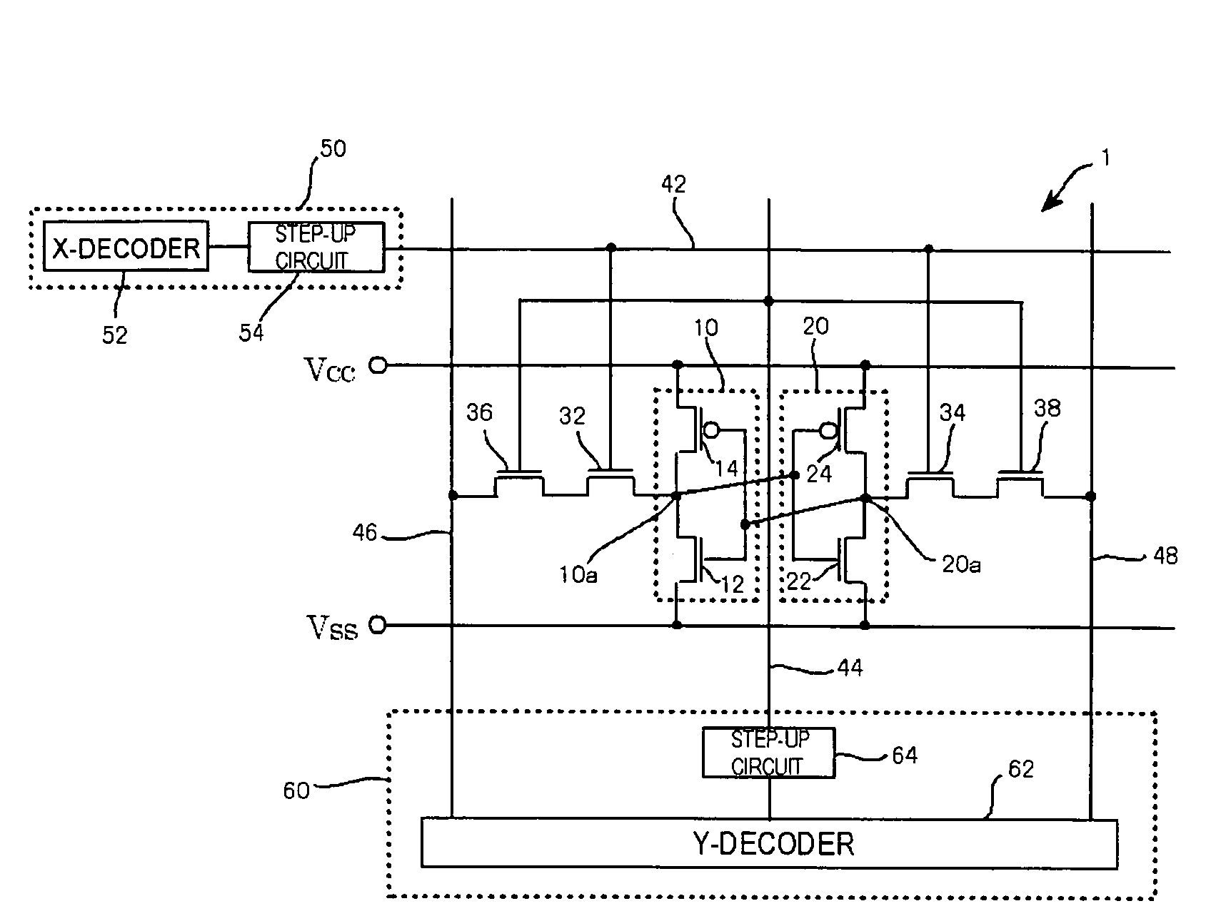
[0018]FIG. 1 is a circuit structure view illustrating an SRAM cell provided in a semiconductor storage device of the first embodiment of the present invention. The semiconductor storage device of this embodiment is an SRAM (Static Random Access Memory) and includes a plurality of SRAM cells 1 shown in the drawing.

[0019]The SRAM cell 1 includes inverters 10, 20, N-type FETs (Field Effect Transistors) 32, 34, 36, 38, word lines 42, 44, bit lines 46, 48, and voltage applying circuits 50, 60. The inverters 10, 20 mutually intersect and are coupled, and constitute a latch circuit. Namely, the output terminal 10a of the inverter 10 (first inverter) and the input terminal of the inverter 20 (second inverter) are connected, and the input terminal of the inverter 10 and the output terminal 20a of the inverter 20 are connected.

[0020]The inverter 10 is composed of an N-type FET 12 (first drive transistor) and a P-type FET 14 (first load transistor). Similarly, the inverter 20 is composed of an...

second embodiment

[0035]FIG. 3 is a circuit structure view illustrating an SRAM cell provided in a semiconductor storage device of the second embodiment of the present invention. The semiconductor storage device of this embodiment is an SRAM and includes a plurality of SRAM cells 2 shown in the drawing. The SRAM cell 2 includes the inverters 10, 20, the N-type FETs 32, 34, 36, 38, the word lines 42, 44, the bit lines 46, 48, and the voltage applying circuit 50. The configuration of each of these elements is the same as for that shown in FIG. 1.

[0036]Further, SRAM cell 2 includes P-type FETs 37, 39 and an inverter 72. The FET 37 (fifth pass transistor) is connected in parallel with the FET 36 and constitutes a CMOS switch together with the FET 36. Specifically, the source and drain of the FET 37 are connected to the source and drain of the FET 36, respectively. Further, the gate of the FET 37 is connected to the word line 44 via the inverter 72.

[0037]Similarly, the FET 39 (sixth pass transistor) is co...


PUM


Abstract

An SRAM cell 1 includes inverters 10, 20, N-type FETs 32, 34, 36, 38, word lines 42, 44, bit lines 46, 48, and voltage applying circuits 50, 60. The voltage applying circuits 50, 60 apply a voltage Vdd to the word lines 42, 44 at the time of a read operation of the SRAM cell 1. The voltage applying circuits 50, 60 apply a voltage (Vdd+α) to the word lines 42, 44 at the time of a write operation of the SRAM cell 1. Here, α>0. Namely, the SRAM cell 1 is configured in such a manner that a voltage applied to word lines 42, 44 at the time of the write operation is higher than at the time of the read operation.

Description

[0001]This application is based on Japanese patent application No. 2005-021126, the content of which is incorporated hereinto by reference.BACKGROUND[0002]1. Technical Field[0003]The present invention relates to a semiconductor storage device.[0004]2. Related Art[0005]Semiconductor storage devices of the related art are disclosed, for example, in Japanese Laid-open Patent Publication NO's H 11-7776, H8-7574, and H10-27476. The semiconductor storage device disclosed in Japanese Laid-open Patent Publication NO. H11-7776 is equipped with an SRAM cell constructed from six transistors. Namely, in addition to four transistors constituting a latch circuit, the SRAM cell also has two pass transistors provided between the latch circuit and bit lines on either side.[0006]With semiconductor storage devices configured in this manner, since a plurality of SRAM cells are controlled by a single word line, cells other than a target cell are selected when a certain word line is selected. This means ...

Claims


Application Information

Patent Timeline
Patent Type & Authority Patents(United States)
IPC IPC(8): G11C11/00G11C8/00
CPCG11C8/08G11C11/413
Inventor ASAYAMA, SHINOBUKOMURO, TOSHIO
Owner RENESAS ELECTRONICS CORP
Why Eureka
Try Eureka