Memory device and method of operation of such a memory device

Active Publication Date: 2015-03-03
ARM LTD
View PDF1 Cites 22 Cited by
  • Summary
  • Abstract
  • Description
  • Claims
  • Application Information

AI Technical Summary

Benefits of technology

[0025]In contrast to the write multiplexing driver circuitry, it should be noted that the read multiplexing driver circuitry asserts the read mux control signal at the peripheral voltage level. Further, since the bit lines are precharged to the peripheral voltage level, the data as sensed by the sense amplifier circuitry can be returned as read data to the peripheral voltage domain without any

Problems solved by technology

The level up shifting mechanism 40 is generally more problematic to implement than the level down shifting mechanism 50 (in fact in many instances no specific level down shifting circuitry may be required), since when performing level up shifting there is the potential for establishing various DC paths that can result in signi

Method used


Image

  • Memory device and method of operation of such a memory device
  • Memory device and method of operation of such a memory device
  • Memory device and method of operation of such a memory device

Examples


Embodiment Construction

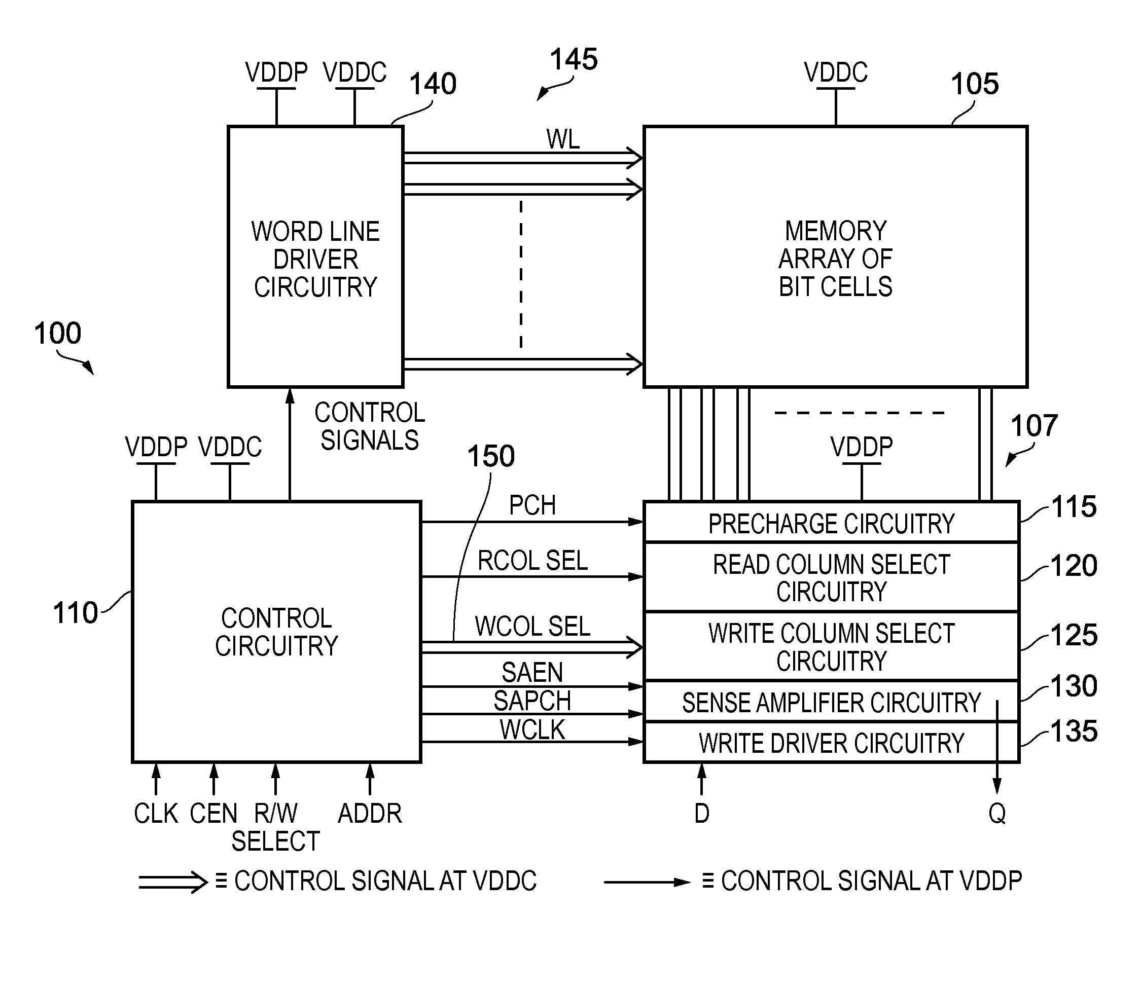
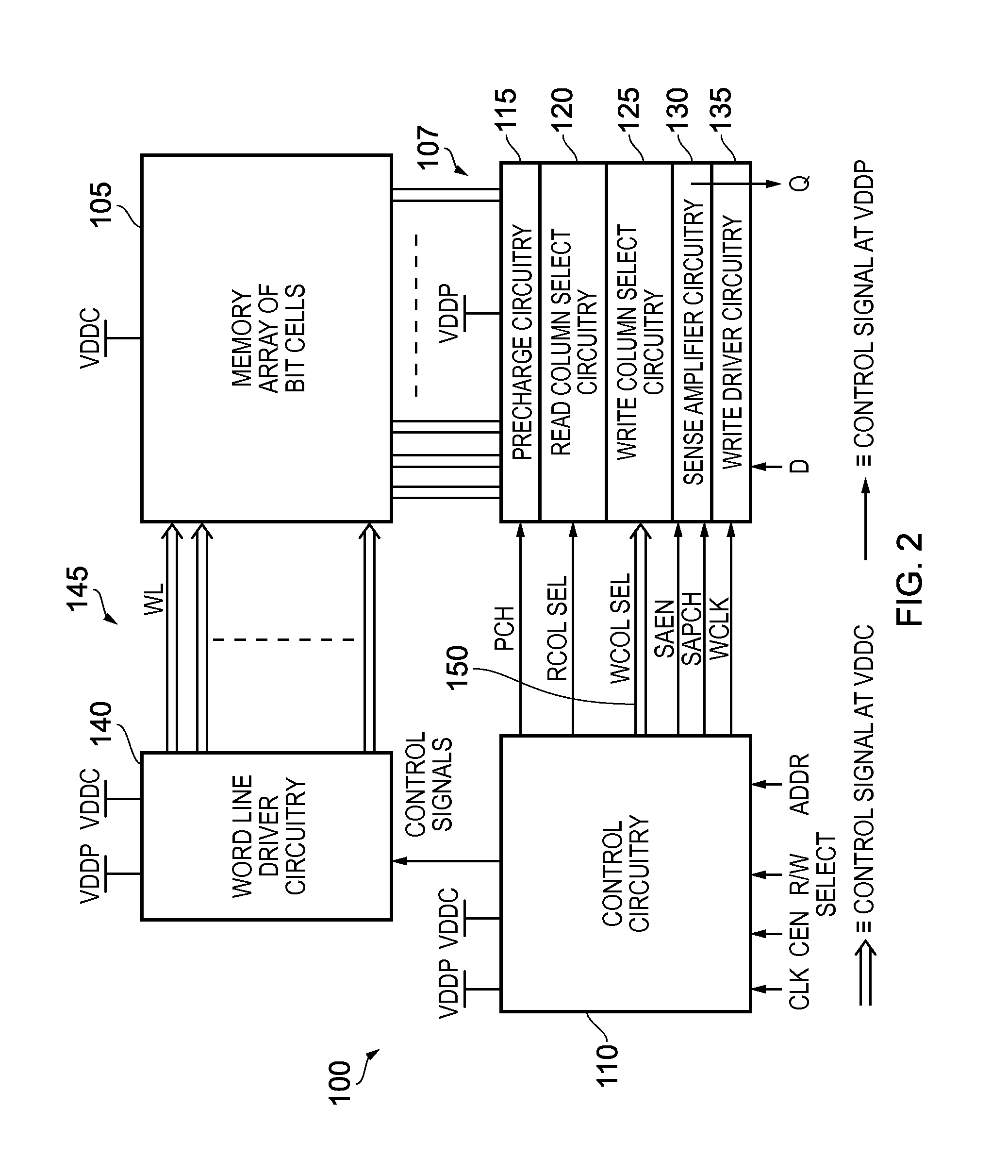
[0041]FIG. 2 is a diagram schematically illustrating a logical arrangement of a memory device in accordance with one embodiment. In particular, the memory device 100 includes a memory array 105 comprising an array of memory cells arranged in a plurality of rows and columns. A plurality of word lines 145 are provided through the array in order to allow individual rows of memory cells to be addressed by the word line driver circuitry 140 during write and read operations. In addition, a plurality of bit lines are provided in association with the columns of memory cells, in this embodiment each column having an associated pair of bit lines, to enable data to be written into an addressed memory cell of that column during a write operation, and for data to be read from an addressed memory cell of that column during a read operation.

[0042]Precharge circuitry 115 is used to precharge the voltage level on the bit lines under the control of control circuitry 110. Following the precharge opera...


PUM


Abstract

A memory device having an array of memory cells connected to a core voltage level, and access circuitry used to perform a write operation in order to write data into a plurality of addressed memory cells. At least one bit line associated with at least each column in the array containing an addressed memory cell is precharged to the peripheral voltage level prior to the write operation being performed. Word line driver circuitry is then configured to assert a word line signal at the core voltage level on the word line associated with the row of the array containing the addressed memory cells. Write multiplexing driver circuitry asserts a mux control signal to write multiplexing circuitry which then couples the bit line of each addressed memory cell to the write driver circuitry in dependence on the mux control signal identifying which column contains the addressed memory cells.

Description

BACKGROUND OF THE INVENTION[0001]1. Field of the Invention[0002]The present invention relates to a memory device and to a method of operation of such a memory device, and in particular to a mechanism for operating such a memory device when the access circuitry used to access the array of memory cells is operated from a peripheral voltage domain with a supply voltage less than the supply voltage in a core voltage domain used by the array of memory cells.[0003]2. Description of the Prior Art[0004]In modern data processing systems, it is becoming more and more common for certain parts of the data processing system to operate in a different voltage domain to one or more other parts. For example, a trend within integrated circuits is the increasingly common use of embedded memory, such as SRAM memory. With the reduction in size of process geometries, the individual memory cells within the memory are becoming less stable. To reduce the power consumption of the integrated circuit, it is de...

Claims


Application Information

Patent Timeline
IPC IPC(8): G11C7/10G11C7/22G06F17/50G11C7/12
CPCG11C7/12G06F17/505G06F2217/78G11C7/1096G11C8/10G11C11/413G11C11/418G11C11/419G11C16/08H03K17/005
Inventor ZHENG, BOKWON, JUNGTAEYEUNG, GUSCHONG, YEW KEONG
Owner ARM LTD
Why Eureka
Try Eureka