Semiconductor integrated circuit

a technology of integrated circuits and semiconductors, applied in logic circuits, logic circuits, logic functions, etc., can solve problems such as impairment of the speed of operation, malfunction of conventional dynamic flip-flop circuits, and inability to perform data selection functions, so as to reduce power consumption and suppress needless operation

Inactive Publication Date: 2007-10-16
PANASONIC CORP
View PDF5 Cites 10 Cited by
  • Summary
  • Abstract
  • Description
  • Claims
  • Application Information

AI Technical Summary

Benefits of technology

[0011]An object of the present invention is to provide a dynamic flip-flop circuit with a data selection function which can operate normally while securing a satisfactorily high-speed operation even when none of a plurality of pieces of data is selected.
[0012]To achieve the object, according to the present invention, when none of a plurality of pieces of data is selected, for example, the precharge of the node N2 is prevented from being discharged of FIG. 3A, so that the H value of the node N2 is maintained. The holding circuit holds and outputs the H value of the node N2.
[0013]A semiconductor integrated circuit of the present invention receives a clock, a plurality of pieces of data, and a plurality of selection signal for selecting the data, and when the clock is transitioned, outputs a selected one of the pieces of data selected by the selection signal to a holding circuit. The semiconductor integrated circuit comprises a non-selected state detection circuit of detecting that all of the plurality of selection signals selects none of the plurality of pieces of data. In the non-selected state detection circuit, when it is detected that all of the plurality of selection signals selects none of the plurality of pieces of data, the previously selected data is prevented from being changed, thereby holding output data of the holding circuit.
[0061]In addition, according to the present invention, when the input data matches a value of the output signal of the holding circuit, an operation of the holding circuit or the like can be stopped. As a result, a needless operation can be suppressed, thereby reducing power consumption.

Problems solved by technology

However, it was found that the conventional dynamic flip-flop circuit having the data selection function malfunctions when none of the plurality of pieces of data is selected.
Therefore, an extra setup time (a time required for the static circuit to establish its output by a rising time of the clock CLK) is required, resulting in impairment of the speed of operation.

Method used


Image

  • Semiconductor integrated circuit
  • Semiconductor integrated circuit
  • Semiconductor integrated circuit

Examples


example 1

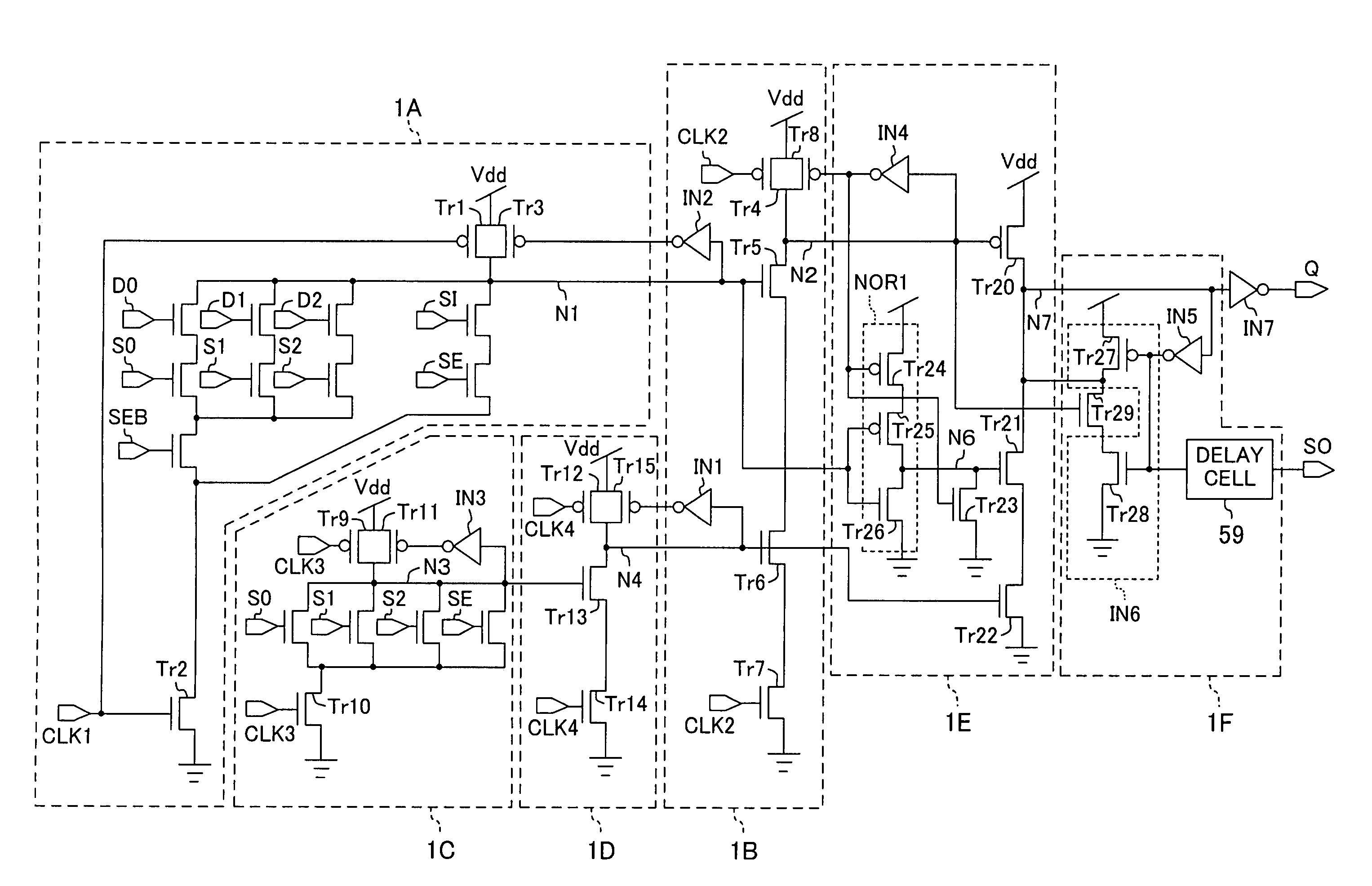
[0085]FIG. 1 illustrates a semiconductor integrated circuit according to Example 1 of the present invention.

[0086]In FIG. 1, D0, D1 and D2 indicate data; S0, S1 and S2 indicate selection signals which are used to select the data D0 to D2, respectively; SI indicates a data input when scanning is performed; SE indicates a scan shift control signal which is used to perform a scan shift operation; SEB indicates an inverted signal of the scan shift control signal; and Q and SO indicate output terminals.

[0087]The semiconductor integrated circuit of FIG. 1 has a first dynamic circuit 1A of NOR type, a second dynamic circuit 1B of NAND type, a third dynamic circuit 1C of NOR type, a fourth dynamic circuit 1D of NAND type, an output circuit 1E, and a holding circuit 1F. The output circuit 1E and the holding circuit 1F constitute a dynamic flip-flop circuit.

[0088]The first dynamic circuit 1A of NOR type receives the three pieces of data D0 to D2, the three selection signals S0 to S2, and a fi...

example 2

[0120]Next, Example 2 of the present invention will be described. In Example 2, the output circuit 1E of FIG. 1 is modified as shown in FIG. 5.

[0121]Specifically, an output circuit 1G of FIG. 5 is composed of a differential circuit 70. More specifically, the differential circuit 70 has a pair of differential input terminals 70a and 70b, a pair of differential output terminals 70c and 70d, two p-type MOS transistors Tr30 and Tr31 and two n-type MOS transistors Tr32 and Tr33 which are cross-linked, and two n-type MOS transistors Tr34 and Tr35 for receiving a differential signal, to whose gates the differential input terminals 70a and 70b are connected. The differential output terminals 70c and 70d are connected to a connection point of the p-type transistor Tr30 and the n-type transistor Tr32 and a connection point of the p-type transistor Tr31 and the n-type transistor Tr33, respectively. The differential output terminals 70d and 70c are the output terminal Q and its inverted output ...

example 3

[0128]FIG. 8 illustrates a semiconductor integrated circuit according to Example 3 of the present invention.

[0129]The semiconductor integrated circuit of Example 3 is different from the semiconductor integrated circuit of FIG. 1 in an NOR type first dynamic circuit 2A and an NOR type third dynamic circuit 2C, and both the circuits have the same second and fourth dynamic circuits 1B and 1D, output circuit 1E and holding circuit 1F.

[0130]In the first dynamic circuit 2A, the p-type transistor Tr1 and the n-type transistor Tr2 are connected in series. To this series circuit, an n-type MOS transistor Tr80 which receives data D through the gate thereof, and another n-type MOS transistor Tr81 which receives an inverted signal NQ of the output signal Q through the gate thereof are connected in series. Therefore, in the first dynamic circuit 2A, the potential of the first output Node N1 is basically determined, depending on the value of the data D. When the data D is output through the outpu...


PUM


Abstract

In a dynamic flip-flop circuit with a data selection function, for example, when data having an H value is selected using a selection signal, a first node N1 is L, a second node N2 of a second dynamic circuit is H, so that an output signal has an H level. In this case, when none of a plurality of pieces of data is selected using a selection signal, the first node N1 is H, so that the electric charge of the second node N2 is discharged and the output signal erroneously has an L level. However, in this case, an output node N3 is H and a fourth node N4 is L, so that an n-type transistor of the second dynamic circuit is turned OFF, thereby preventing the second node N2 from being discharged. Therefore, a normal operation is performed while securing a satisfactorily high-speed operation even when none of the pieces of data is selected.

Description

CROSS REFERENCE TO RELATED APPLICATIONS[0001]This Non-provisional application claims priority under 35 U.S.C. §119(a) on Patent Application No. 2004-218244 filed in Japan on Jul. 27, 2004, the entire contents of which are hereby incorporated by reference. The entire contents of Patent Application No. 2005-194608 filed in Japan on Jul. 4, 2005 are also incorporated by reference.BACKGROUND OF THE INVENTION[0002]The present invention relates to a semiconductor integrated circuit, and more particularly, to a high-speed semiconductor integrated circuit.[0003]Conventionally, the speed of a semiconductor integrated circuit, particularly a flip-flop circuit, is increased by incorporating a dynamic circuit into its internal structure as described in, for example, JP No. 2003-060497 A. The dynamic flip-flop circuit described in this publication receives a plurality of pieces of data, selects any one of them, and holds and outputs the selected data.[0004]Hereinafter, the structure of the flip-...

Claims


Application Information

Patent Timeline
Patent Type & Authority Patents(United States)
IPC IPC(8): H03K19/096H03K19/20
CPCH03K3/356139
Inventor SUMITA, MASAYA
Owner PANASONIC CORP
Why Eureka
Try Eureka