Secure digital memory card using land grid array structure

a secure digital memory and land grid array technology, applied in the field of memory cards, can solve the problems of increasing the manufacturing cost of the prior art memory card, increasing the susceptibility of internal components mounted to the substrate to being contaminated with various particles, and decreasing the yield rate, so as to achieve complex signal routing

Active Publication Date: 2007-11-13
AMKOR TECH SINGAPORE HLDG PTE LTD
View PDF38 Cites 55 Cited by
  • Summary
  • Abstract
  • Description
  • Claims
  • Application Information

AI Technical Summary

Benefits of technology

[0010]In accordance with the present invention, there is provided a memory card which includes a land grid array (LGA) structure and is fabricated such that the external signal contacts (ESC's) are located on or about the same plane as the bottom side or surface of the memory card, and the exposed tie bars which are typical artifacts of traditional leadframe based memory cards are eliminated. The molding process used in the fabrication of the memory card of the present invention also effectively eliminates the need for the separate cap or lid of prior art memory cards, and provides a molded memory card with the desirable look of a lidded memory card. Further, the land grid array structure in the present memory card provides signal routing capability similar to that of a laminate substrate of a conventional memory card, but provides many of the cost / manufacturing economies of currently known leadframe based memory cards. In addition to eliminating the exposed tie bars and providing more complex signal routing that is required for die stack applications, the land grid array structure of the present memory card provides metal features (e.g., traces, die pads, test points / pads, etc.) which are exposed in the card body and used for interconnects between at least one semiconductor die and SMT (surface mount technology) components. These metal features are ultimately covered by a non-conductive label / ink applied to the card body.
[0011]The elimination of the separate cap or lid in the present memory card lowers manufacturing costs while increasing yield rate. Moreover, the completed memory card is devoid of any exposed metal features other than for the external signal contacts thereof. Further, as indicated above, the land grid array substrate in the present memory card provides signal routing capability similar to that of a laminate substrate of a conventional memory card, but provides many of the cost / manufacturing economies of currently known leadframe based memory cards. Thus, the memory card of the present invention possesses the most desirable attributes of both laminate based, lidded memory cards and leadframe based, molded memory cards.

Problems solved by technology

The cap is typically fabricated such that when mounted to the substrate, the resultant memory card meets or achieves a desired “form factor.” As will be recognized, the requirement of separately fabricating the cap and thereafter carrying out a separate process or step to mechanically couple the cap to the substrate increases the manufacturing cost for the prior art memory card, in addition to decreasing yield rate.
This separate coupling process also increases the susceptibility of the internal components mounted to the substrate of being contaminated with various particles.
Though leadframe based memory cards possess certain advantages over circuit board based cards, one of the drawbacks associated with leadframe based memory cards is that portions of the tie bars which are used to connect the contacts and / or die pad(s) of the leadframe to the outer frame thereof are typically exposed in the leading edge and remaining side edges of the memory card.
These exposed portions of the tie bars give rise to a potential to short against the metal features of the host socket, and are thus highly undesirable.
Another limitation of the leadframe based memory card is routability.
Leadframe based memory cards cannot accommodate complex component interconnections.

Method used


Image

  • Secure digital memory card using land grid array structure
  • Secure digital memory card using land grid array structure
  • Secure digital memory card using land grid array structure

Examples


Embodiment Construction

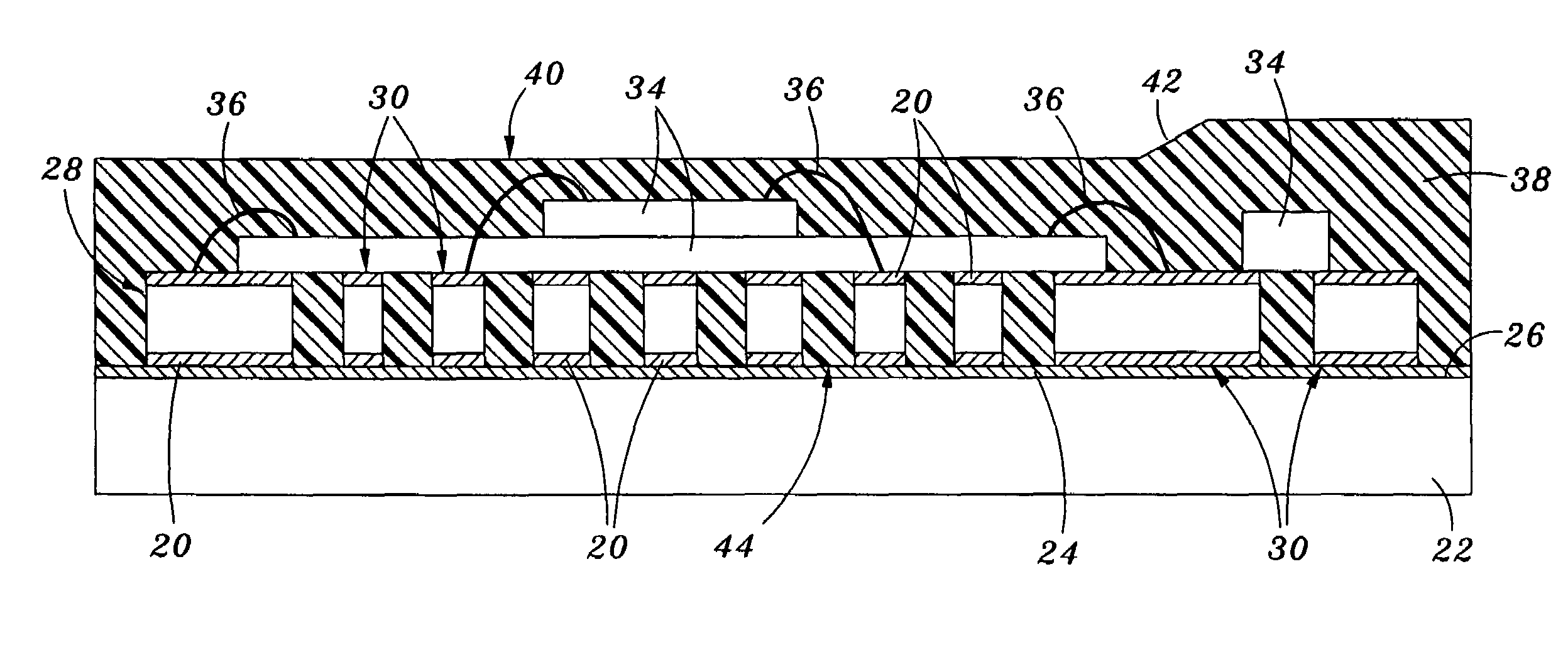
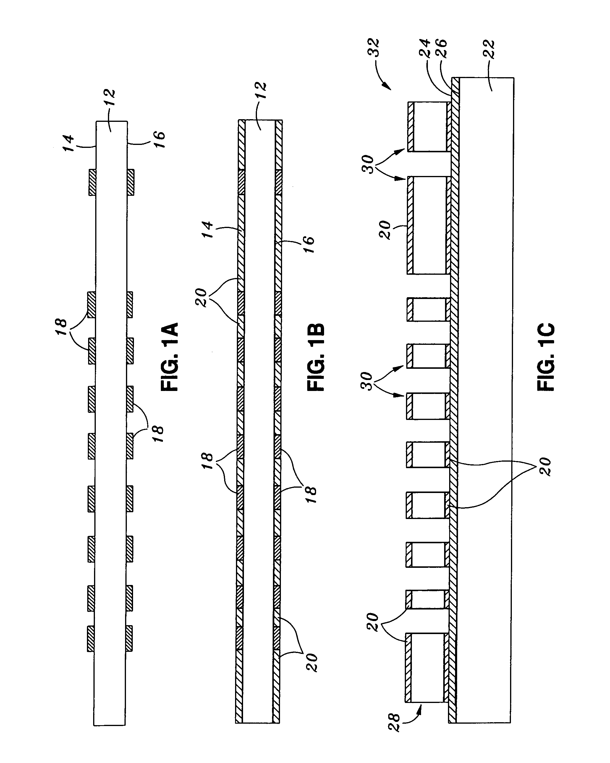
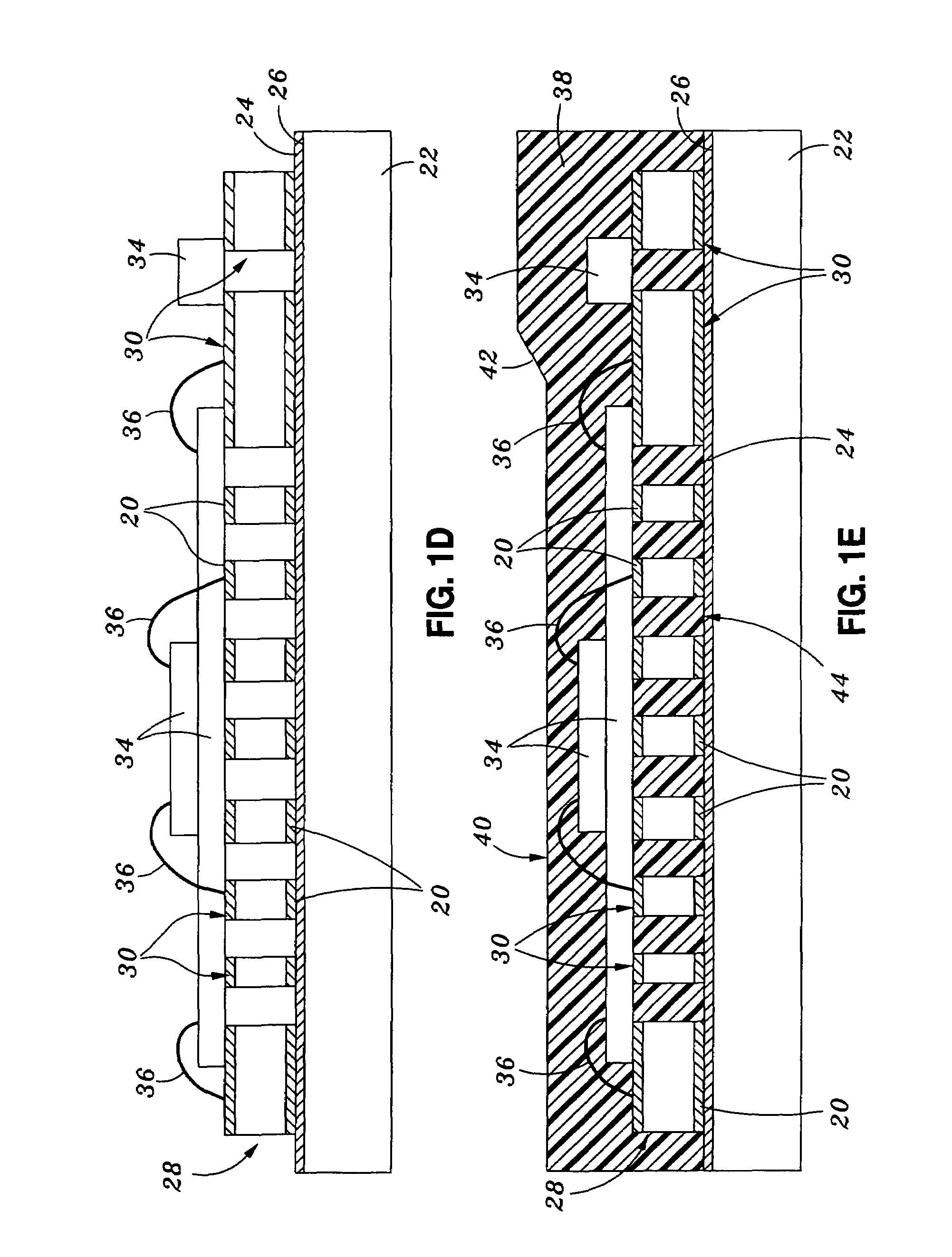
[0020]Referring now to the drawings wherein the showings are for purposes of illustrating preferred embodiments of the present invention only, and not for purposes of limiting the same, FIGS. 1A-1E illustrate an exemplary sequence of steps which may be used to facilitate the formation of a memory card 10 which is constructed in accordance with the present invention and shown in its completed state in FIGS. 4 and 5. Those of ordinary skill in the art will recognize that the fabrication process which will be described below, though applicable to fabricate one memory card 10 at a time, is typically implemented on a scale wherein multiple memory cards 10 are simultaneously fabricated using a common carrier / substrate. As shown in FIG. 1A, in the initial step of the fabrication process for the memory card 10, a layer or sheet 12 of a conductive metal material (e.g., copper) is provided, the sheet 12 defining a generally planar first (top) surface 14 and an opposed, generally planar second...


PUM


Abstract

A memory card comprising a substrate which has a plurality of contacts and a plurality of metal features. The contacts and the metal features are disposed in spaced relation to each other and each define opposed first and second surfaces. Mounted to the substrate is at least one electronic component which is electrically connected thereto. A body covers the electronic component and at least portions of the contacts and the metal features such that the second surfaces of the contacts and the metal features are exposed in a common exterior surface of the body.

Description

CROSS-REFERENCE TO RELATED APPLICATIONS[0001]The present application is a continuation-in-part of U.S. application Ser. No. 11 / 060,264 entitled SECURE DIGITAL MEMORY CARD USING LAND GRID ARRAY STRUCTURE filed Feb. 17, 2005 now U.S. Pat. No. 7,112,875, the disclosure of which is incorporated herein by reference.STATEMENT RE: FEDERALLY SPONSORED RESEARCH / DEVELOPMENT[0002]Not ApplicableBACKGROUND OF THE INVENTION[0003]The present invention relates generally to memory cards, and more particularly, to a memory card (e.g., a secure digital card (SDC)) which includes a land grid array (LGA) structure and is fabricated such that the external signal contacts (ESC's) are located on or about the same plane as the bottom side or surface of the memory card, and the exposed tie bars which are typical artifacts of traditional leadframe based memory cards are eliminated without compromising routability between the components.[0004]As is well known in the electronics industry, memory cards are being...

Claims


Application Information

Patent Timeline
Patent Type & Authority Patents(United States)
IPC IPC(8): G06K19/06
CPCH01L21/561H01L21/568H01L21/6835H01L23/3135H01L24/97H01L2224/48091H01L2924/01033H01L2924/01006H01L2224/48247H01L2224/97H01L2924/01027H01L2924/01029H01L2924/01047H01L2924/01075H01L2924/01078H01L2924/01079H01L2924/01082H01L2924/14H01L2924/19105H01L2924/3025H01L24/48H01L2924/01005H01L2224/85H01L2924/00014H01L2924/181H01L2924/00012H01L2224/45099H01L2224/45015H01L2924/207
Inventor MIKS, JEFFREY ALAN
Owner AMKOR TECH SINGAPORE HLDG PTE LTD
Why Eureka
Try Eureka