Semiconductor device including a vertical field effect transistor, having trenches, and a diode

a vertical field effect transistor and diode technology, applied in the field of semiconductor devices, can solve the problems that the diode formed of polycrystalline silicon cannot operate in a high temperature environment, the field effect transistor using silicon carbide cannot be applied to any high temperature environment, and cannot be used as the temperature sensor

Active Publication Date: 2007-12-11
HITACHI LTD +1
View PDF10 Cites 277 Cited by
  • Summary
  • Abstract
  • Description
  • Claims
  • Application Information

AI Technical Summary

Benefits of technology

[0012]In another preferable implementation aspect of the present invention, a fifth layer of the second conductivity type is formed along the second surface of the semiconductor substrate between the field effect transistor and the diode. An electrode is joined to the fifth layer, and grounded. As a result, separation is conducted so as to prevent a high voltage applied to a first surface of the semiconductor substrate from being applied to the built-in diode, and the separation portion is grounded.
[0013]In a desirable implementation aspect of the present invention, typically pinch-off is caused by control layers respectively disposed along the trenches. Therefore, a voltage applied to a first surface of the semiconductor substrate does not affect the diode. As a result, a diode capable of operating up to a high temperature can be obtained on the same substrate as the field effect transistor.
[0014]In another desirable implementation aspect of the present invention, a voltage applied to a first surface of the substrate is prevented by the deep third layer of the second conductivity type p (or n) from affecting the diode disposed inside the third layer. As a result, a diode capable of operating up to a high temperature can be obtained on the same substrate as the field effect transistor.

Problems solved by technology

However, field effect transistors using silicon carbide cannot be applied to any high temperature environment.
However, the diode formed of polycrystalline silicon does not operate in a high temperature environment anticipated in the case of silicon carbide, and it cannot be used as the temperature sensor.

Method used


Image

  • Semiconductor device including a vertical field effect transistor, having trenches, and a diode
  • Semiconductor device including a vertical field effect transistor, having trenches, and a diode
  • Semiconductor device including a vertical field effect transistor, having trenches, and a diode

Examples


first embodiment

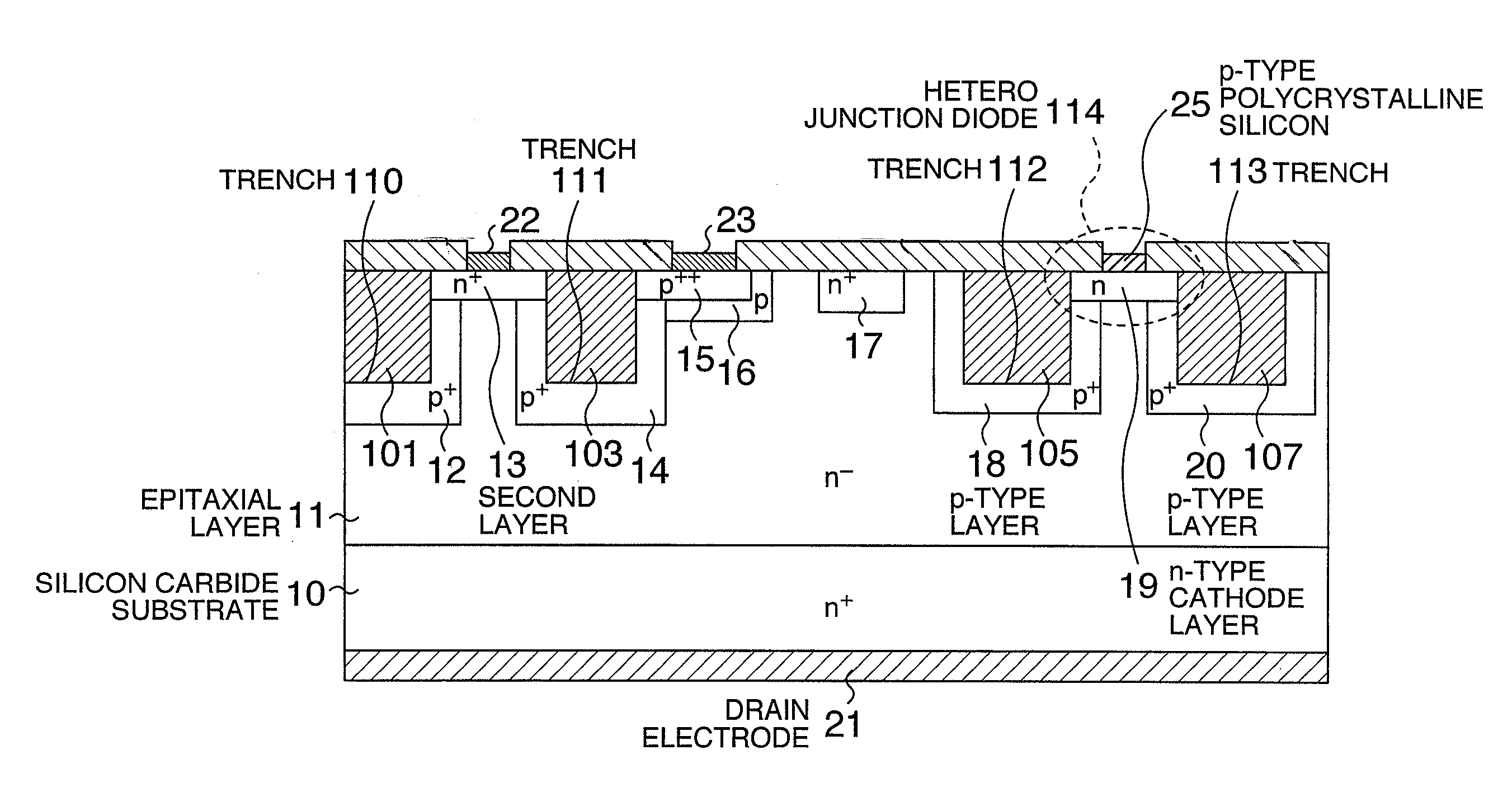
[0036]FIG. 1 is a longitudinal section view of a semiconductor device according to the present invention. A silicon carbide semiconductor substrate having a band gap of at least 2.0 eV includes a semiconductor substrate 10 of a first conductivity type n (or p), and an epitaxial layer 11 of the same first conductivity type n (or p) adjacent to the first layer 10, successively from a first surface side thereof (bottom of FIG. 1). Hereafter, the first conductivity type n (or p) is simply referred to as n-type and the second conductivity type p (or n) is simply referred to as p-type.

[0037]Deep trenches 110 and 111 are formed from a second surface side (top side in FIG. 1). These trenches are filled with insulation films 101 and 103, respectively. There are p-type control regions 12 and 14 along side walls of the trenches 110 and 111, respectively. There is a source region 13 along the second surface of a region sandwiched between the two adjacent trenches 110 and 111. A static induction...

second embodiment

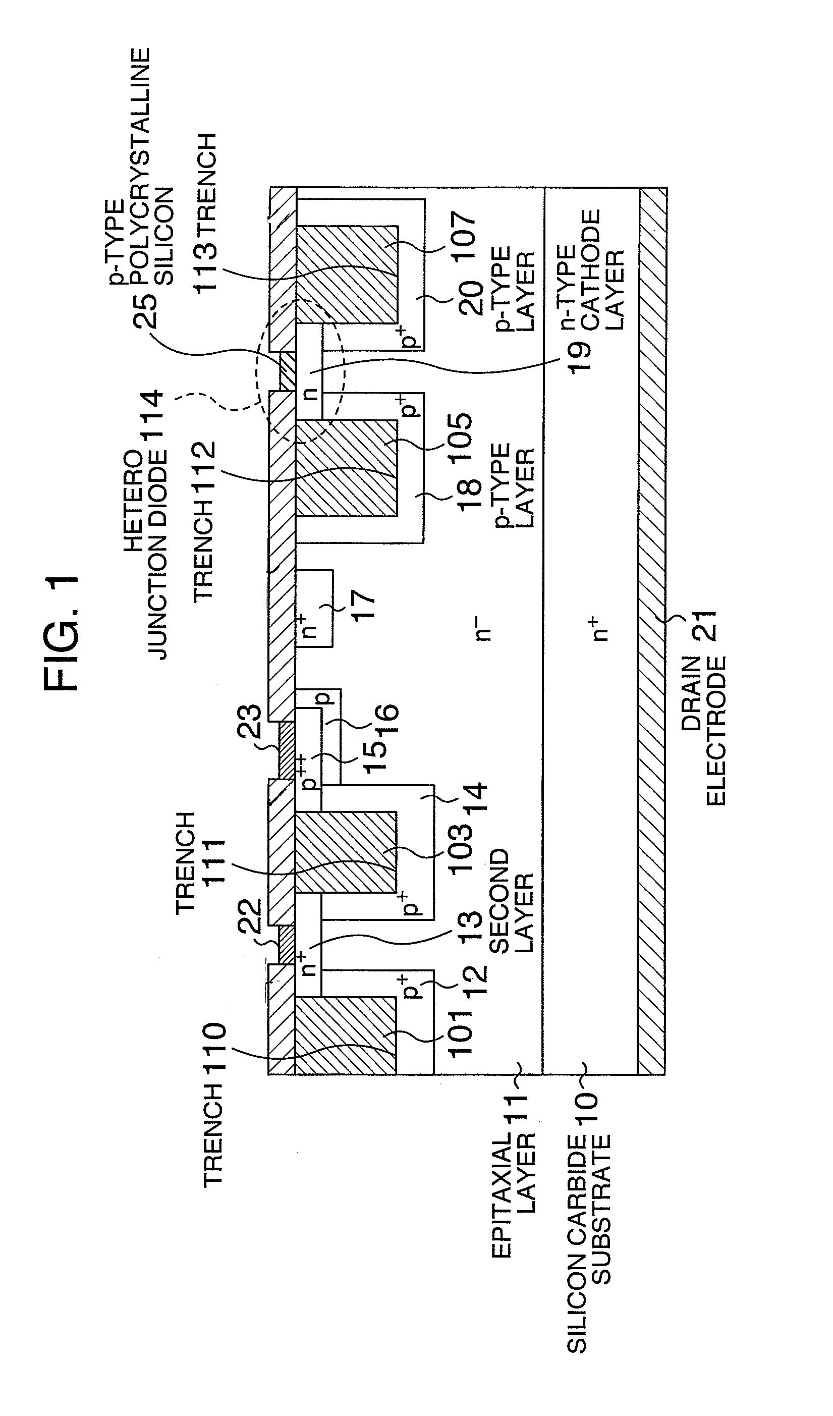
[0042]FIG. 2 is a longitudinal section view of a semiconductor device according to the present invention. There are trenches 110 and 111 on silicon carbide having an n-type semiconductor substrate 10 and an n-type epitaxial layer 11. The trenches 110 and 111 are filled with insulation films 101 and 103, respectively. There are p-type control regions 12 and 14 respectively along side walls of the trenches 110 and 111. There is a source region 13 along the second surface of a region sandwiched between the two adjacent trenches 110 and 111. A static induction transistor including a drain electrode 21, a source electrode 22 and a gate electrode 23 is thus constituted. A p-type layer 16 is a p-type control layer field limiting portion, and an n-type layer 17 is a punch-through stopper layer. The configuration heretofore described is the same as that in FIG. 1. Hereafter, the same portions as those in FIG. 1 are denoted by like reference numerals, and duplicated description will be avoide...

third embodiment

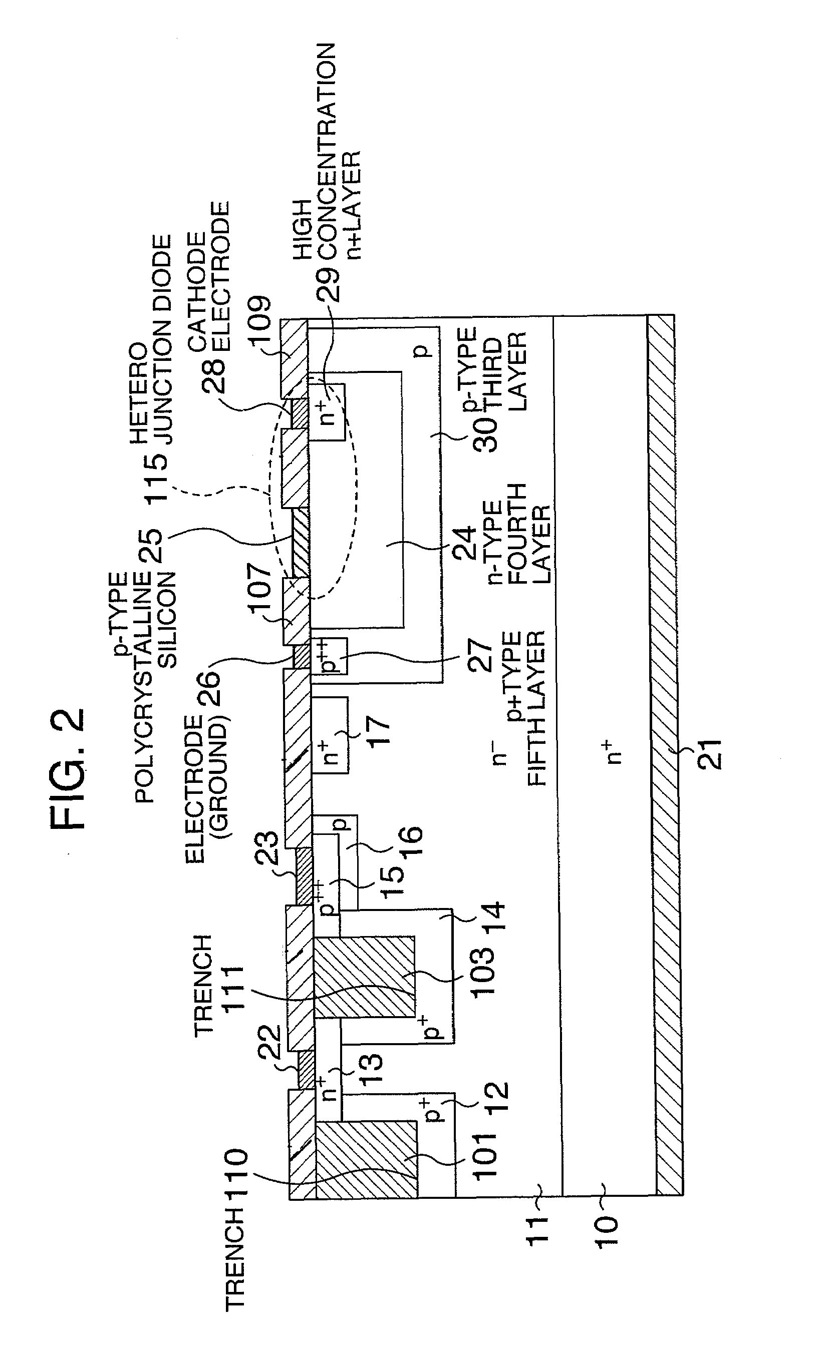
[0048]FIG. 3 is a longitudinal section view of a semiconductor device according to the present invention. Hereafter, the same portions as those in FIG. 1 are denoted by like reference numerals, and duplicated description will be avoided. Only different configurations will be described. The semiconductor device includes an n-type cathode layer 19 in a region sandwiched between the two adjacent trenches 112 and 113. The semiconductor device includes a p-type anode layer 32 inside the n-type cathode layer 19, and an anode electrode 31 in ohmic contact with the p-type anode layer 32. The p-type anode layer 32 and the anode electrode 31 serve as an anode portion and its electrode of a p-n junction diode 116. In the depth direction shown in FIG. 3, the p-type anode layer 32 and the anode electrode 31 do not exist in as far as the deepest portion. In the deepest portion, a cathode electrode (not illustrated) of the p-n junction diode 116 is formed in ohmic contact with the n-type cathode l...


PUM


Abstract

A semiconductor device includes (a) a vertical field effect transistor, the vertical field effect transistor including a drain electrode formed on a first surface of a first conductivity type of a semiconductor, a pair of first trenches formed from a second surface of the semiconductor, control regions of a second conductivity type formed respectively along the first trenches, a source region of the first conductivity type formed along the second surface of the semiconductor between the first trenches, a source electrode joined to the source region, and a gate electrode adjacent to the control regions, (b) a pair of second trenches formed from the second surface of the semiconductor independently of the field effect transistor, (c) control regions of the second conductivity type formed along the second trenches, and (d) a diode having a junction formed on the second surface between the second trenches.

Description

CROSS-REFERENCE TO RELATED APPLICATION[0001]The present application relates to subject matters described in a co-pending patent application Ser. No. 11 / 138,298 filed on May 27, 2005 entitled “SEMICONDUCTOR DEVICES” and assigned to the assignees of the present application. The disclosures of this co-pending application are incorporated herein by reference.BACKGROUND OF THE INVENTION[0002]The present invention relates to a semiconductor device. In particular, the present invention relates to a semiconductor device using silicon carbide.[0003]Because of their excellent properties, field effect transistors using silicon carbide are anticipated to be used in a high temperature environment at a temperature of, for example, at least 150° C., preferably at a temperature of at least 300° C. which cannot be achieved with field effect transistors using silicon.[0004]However, field effect transistors using silicon carbide cannot be applied to any high temperature environment. Since there is an ...

Claims


Application Information

Patent Timeline
Patent Type & Authority Patents(United States)
IPC IPC(8): H01L29/76
CPCH01L29/1066H01L29/8083H01L29/7722
Inventor OHYANAGI, TAKASUMIWATANABE, ATSUOSAKAKIBARA, TOSHIOYAMAMOTO, TSUYOSHINAKAMURA, HIROKIMALHAN, RAJESH KUMAR
Owner HITACHI LTD
Why Eureka
Try Eureka