Method for Producing Virtual Ge Substrates for III/V-Integration on Si(001)

Inactive Publication Date: 2007-10-04
DICHROIC CELL
View PDF9 Cites 284 Cited by
  • Summary
  • Abstract
  • Description
  • Claims
  • Application Information

AI Technical Summary

Benefits of technology

[0032] It is another object of the invention to provide a

Problems solved by technology

The 4% lattice mismatch between GaAs and Si induces, however, large defect densities when GaAs is grown epitaxially on Si, leading to greatly degraded properties (see for example Ahrenkiel et al., J. Electrochem. Soc. 137, 996 (1990), the content of which is incorporated herein by reference).
The class of vapor deposition methods generally called physical vapor deposition suffers from the additional problem of source depletion, as is evident in molecular beam epitaxy (MBE) where electron beam evaporators need to be refilled regularly (see for example Hackbarth et al., Thin Solid Films 369, 148 (2000) the content of which is incorporated herein by reference).
Virtual substrates made from graded Si1-xGex buffer layers suffer from two main disadvantages: (1) they require many micrometers of epitaxial growth for grading rates low enough to ensure low threading dislocation densities, (2) their surfaces are relatively rough, being characterized by the so-called cross-hatch morphology associated with the relaxation process (see for example Lutz et al., Appl. Phys. Lett. 66, 724 (1995), the content of which is incorporated herein by reference).
Because of the large layer thickness epitaxial growth is very time consuming for most prior art techniques.
A common feature of all CVD processes is their relatively inefficient use of expensive source gases, most of which leave the reactor without being decomposed an

Method used


Image

  • Method for Producing Virtual Ge Substrates for III/V-Integration on Si(001)
  • Method for Producing Virtual Ge Substrates for III/V-Integration on Si(001)
  • Method for Producing Virtual Ge Substrates for III/V-Integration on Si(001)

Examples


Embodiment Construction

)

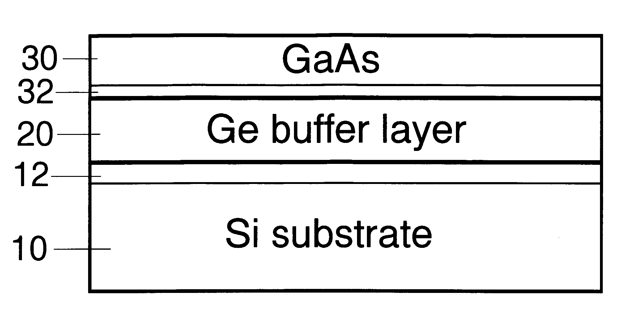
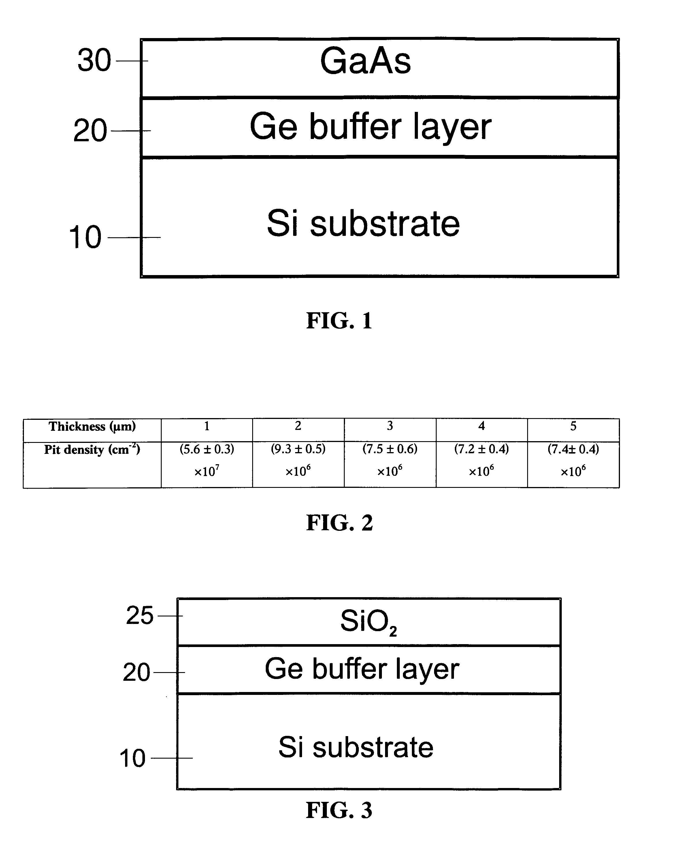
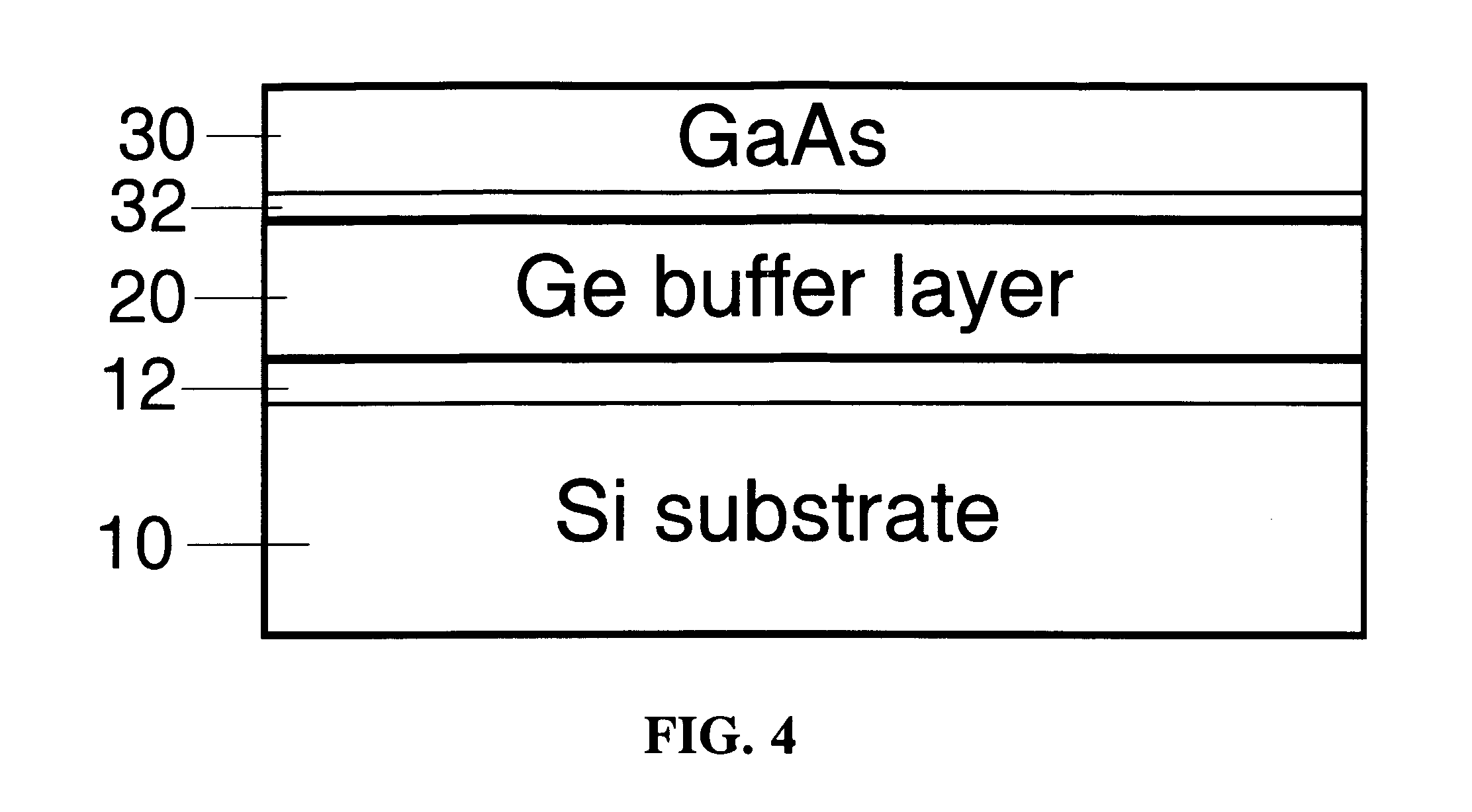
[0043] A first embodiment of the invention is shown in FIG. 1. The surface of a Si wafer 10 is cleaned by a wet chemical treatment or a hydrogen plasma treatment. After loading into the LEPECVD reactor the layout of which has been described for example in U.S. Pat. No. 6,454,855 to von Känel et al., the temperature of the wafer is increased to approximately 600° C. Next, a Ge buffer layer 20 is epitaxially grown by low-energy plasma-enhanced chemical vapor deposition (LEPECVD), preferably at a rate of at least 5 nm / s. The thickness of the Ge layer is preferably chosen to be in the range of 0.75 to 5 μm. It has been shown by high-resolution X-ray diffraction that Ge layers grown in this way are relaxed to 100%. Surface roughness measured by AFM amounts to typically 1 nm rms.

[0044] The temperature is then raised to above 700° C., preferably to about 900° C., for about 10 minutes. In another embodiment of the invention the temperature is repeatedly cycled between about 700° C. and 90...


PUM

PropertyMeasurementUnit
Temperatureaaaaaaaaaa

Abstract

Relaxed germanium buffer layers can be grown economically on misoriented silicon wafers by low-energy plasma-enhanced chemical vapor deposition, in conjunction with thermal annealing and/or patterning, the buffer layers can serve as high-quality virtual substrates for the growth of crack-free GaAs layers suitable for high-efficiency solar cells, lasers and field effect transistors.

Description

BACKGROUND OF THE INVENTION [0001] There have been many attempts to combine the advantages of large, high quality Si substrates with the superior electronic and optical properties of III / V-compound semiconductors, such as GaAs. Monolithic integration of optoelectronic GaAs devices on Si substrates has been a goal for more than two decades (for a review, see for example Mat. Res. Soc. Symp. Proc. 116 (1989), the content of which is incorporated herein by reference). The 4% lattice mismatch between GaAs and Si induces, however, large defect densities when GaAs is grown epitaxially on Si, leading to greatly degraded properties (see for example Ahrenkiel et al., J. Electrochem. Soc. 137, 996 (1990), the content of which is incorporated herein by reference). [0002] In order to reduce defect densities, various kinds of intermediate buffer layers between the Si substrate and the GaAs layer have been devised. The object of these epitaxial buffer layers is to act as virtual substrates (VS) w...

Claims


Application Information

Patent Timeline
IPC IPC(8): C23C16/00H01L21/20H01L21/205
CPCC23C16/0209Y02E10/544C23C16/28C23C16/56H01L21/02381H01L21/02433H01L21/0245H01L21/02463H01L21/02505H01L21/02546H01L21/0262H01L31/0304H01L31/0392H01L2924/10329H01L2924/19042C23C16/0272
Inventor VON KAENEL, HANS
Owner DICHROIC CELL
Why Eureka
Try Eureka