Method of fabricating a gate structure of a field effect transistor having a metal-containing gate electrode

Inactive Publication Date: 2005-01-13
APPLIED MATERIALS INC
View PDF17 Cites 305 Cited by
  • Summary
  • Abstract
  • Description
  • Claims
  • Application Information

AI Technical Summary

Benefits of technology

[0011] In another embodiment, the method is used to fabricate a gate structure of a field effect transistor having a metal-containing gate electrode (e.g., titanium (Ti), tantalum (Ta), tungsten (W), titanium nitride (TiN), tantalum nitride (TaN), tungsten nitride (WN), and the

Problems solved by technology

Etch processes used during fabrication of the gate structures having metal-containing gate electrodes may have low etch selectivity to the underlying dielectric layers and, as such, damage the gate dielectric layer of the transistor.
Removal of the residue using conventional etchants (e.g., chlorine (Cl2), hydrogen bromide (HBr), and the like) is a difficult to control process that may also damage the thin gate dielectric layer, as well as contaminate a pro

Method used


Image

  • Method of fabricating a gate structure of a field effect transistor having a metal-containing gate electrode
  • Method of fabricating a gate structure of a field effect transistor having a metal-containing gate electrode
  • Method of fabricating a gate structure of a field effect transistor having a metal-containing gate electrode

Examples


Embodiment Construction

[0019] The present invention is a method for etching metals (e.g., titanium (Ti), tantalum (Ta), tungsten (W), and the like) and / or metal-containing conductive compounds (e.g., titanium nitride (TiN), tantalum nitride (TaN), tungsten nitride (WN), and the like) with high etch selectivity to underlying dielectric material layers having a dielectric constant of about 4.0 or greater (e.g., silicon dioxide (SiO2), silicon oxynitride (SiON), and the like). The method may be used for fabricating ultra-large-scale integrated (ULSI) semiconductor devices and circuits.

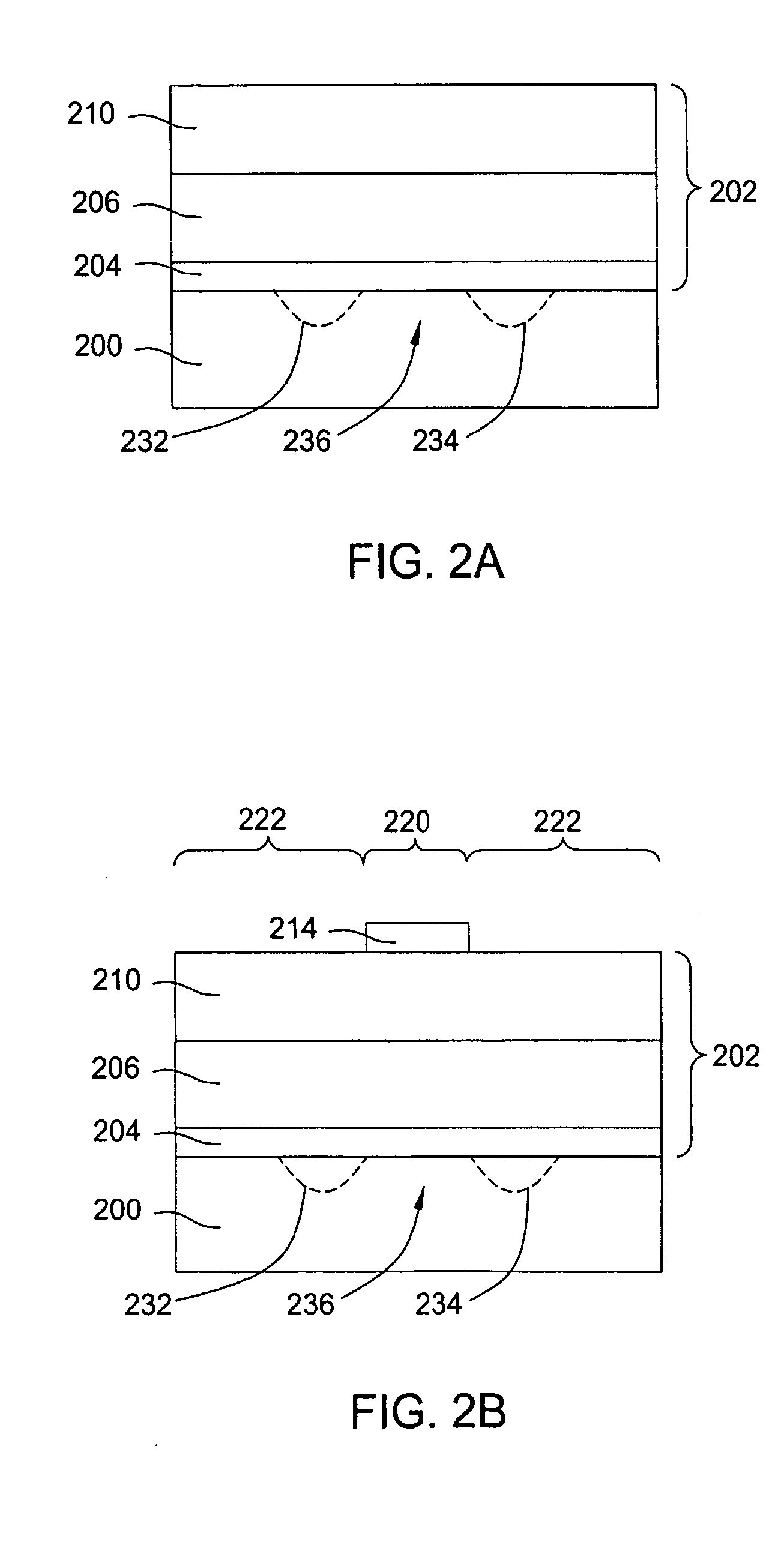
[0020] The present invention also includes a method for fabricating a gate structure of a field effect transistor (e.g., complementary metal-oxide-semiconductor (CMOS) field effect transistor, and the like) comprising a metal-containing gate electrode and an ultra-thin (e.g., about 10 to 20 Angstroms) gate dielectric layer.

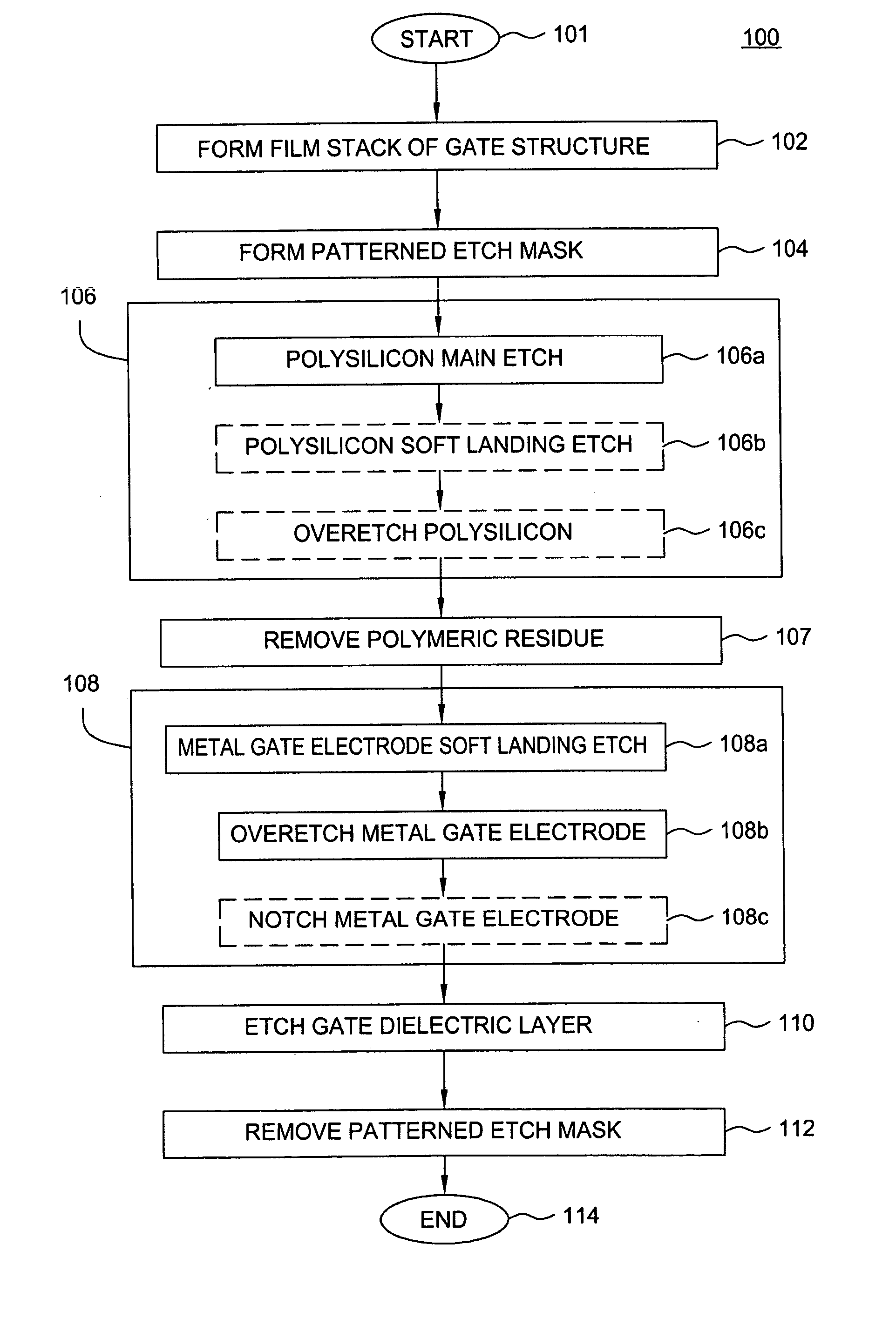
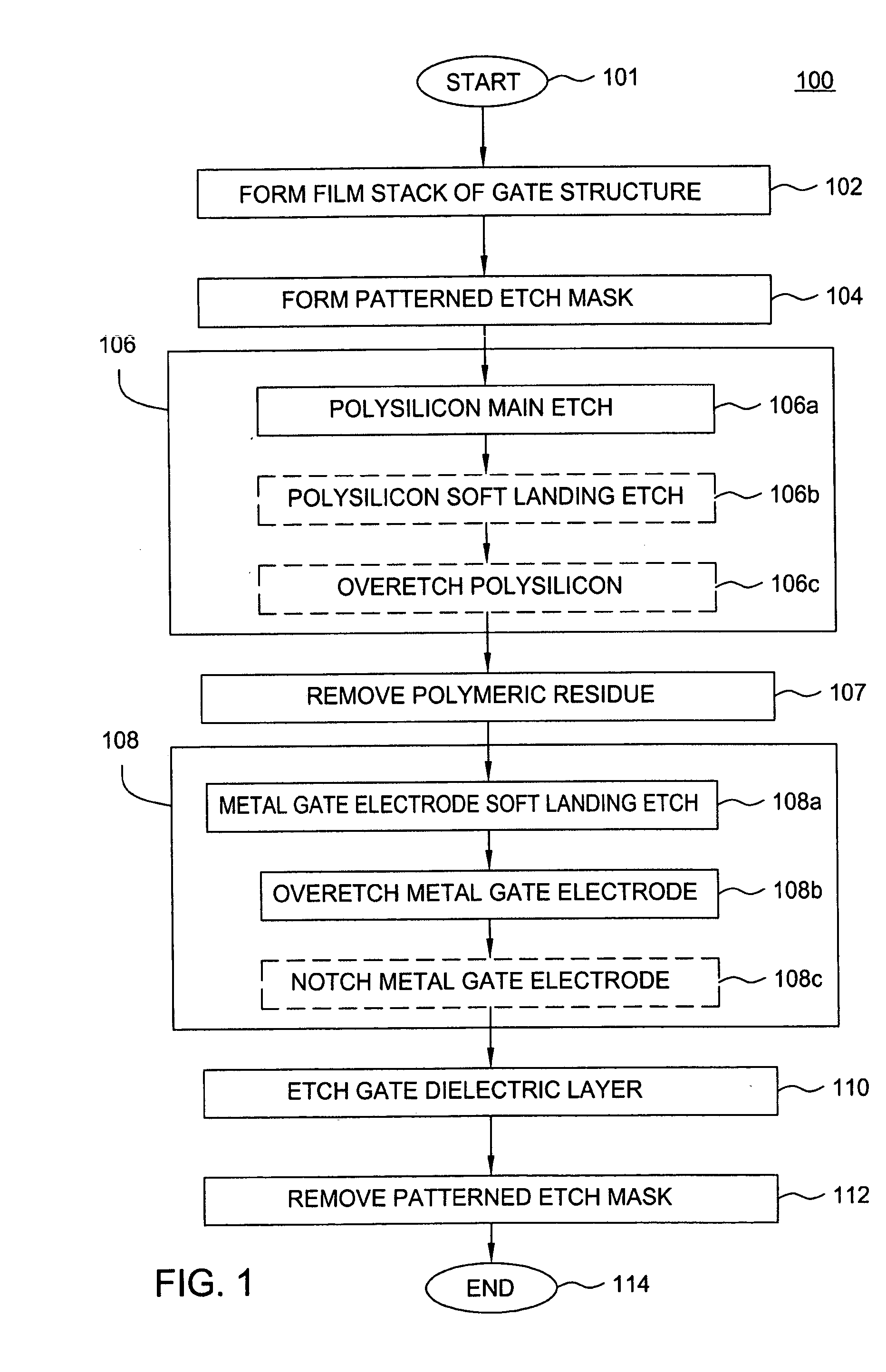
[0021]FIG. 1 depicts a flow diagram for one embodiment of the inventive method for fabricating a gate st...


PUM


Abstract

A method of etching metals and/or metal-containing compounds using a plasma comprising a bromine-containing gas. In one embodiment, the method is used during fabrication of a gate structure of a field effect transistor having a titanium nitride gate electrode, an ultra-thin (about 10 to 20 Angstroms) silicon dioxide gate dielectric, and a polysilicon upper contact. In a further embodiment, the gate electrode is selectively notched to a pre-determined width.

Description

CROSS-REFERENCE TO RELATED APPLICATIONS [0001] This application claims benefit of U.S. Provisional Patent Application Ser. No. 60 / 486,220 filed Aug. 10, 2003, and U.S. Provisional Patent Application Ser. No. 60 / 507,597 filed Sep. 30, 2003, which are herein incorporated by reference.BACKGROUND OF THE INVENTION [0002] 1. Field of the Invention [0003] The present invention generally relates to a method of fabricating devices on semiconductor substrates. More specifically, the present invention relates to a method of fabricating a field effect transistor having a metal-containing gate electrode. [0004] 2. Description of the Related Art [0005] Microelectronic devices are generally fabricated on a semiconductor substrate as integrated circuits wherein various conductive layers are interconnected with one another to facilitate propagation of electronic signals within the device. An example of such a device is a complementary metal-oxide-semiconductor (CMOS) field effect transistor. [0006] ...

Claims


Application Information

Patent Timeline
IPC IPC(8): H01L21/336H01L21/28H01L21/3213H01L21/8238H01L29/78
CPCH01L21/28035H01L21/28123H01L29/78H01L21/32137H01L21/32136Y10S438/942H01L21/18H01L21/8238
Inventor CHOI, JINHANDESHMUKH, SHASHANKYI, SANGLEE, KYEONG-TAE
Owner APPLIED MATERIALS INC
Why Eureka
Try Eureka