[0013]A more specific object of the present invention is to provide a semiconductor device that can set an optimum reference voltage according to changes with age in the internal reference cells, and a method of generating a reference voltage.
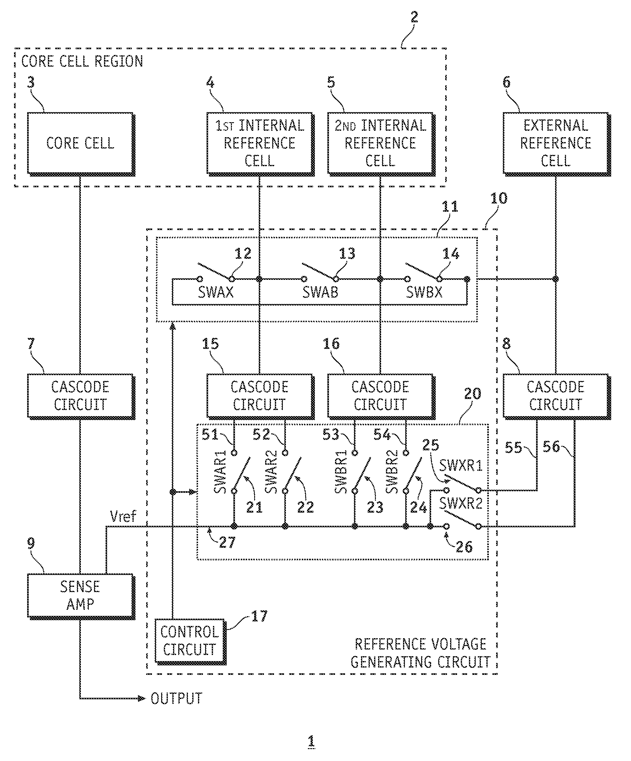
[0014]The above objects of the present invention are achieved by a semiconductor device that includes at least one reference cell, a cascode circuit that has at least two current mirror circuits and outputs voltages dependent on a current flowing through the at least one reference cell to at least two output paths, and a switch that selectively connects the at least two output paths to a given output terminal. With this structure, the number of voltage outputs can be increased and decreased without an increase in the number of reference cells. Accordingly, the reference voltage determined from those voltages can be readily adjusted and reading can be performed without a decrease in margin at the time of data reading from the core cell.
[0015]The above objects of the present invention are also achieved by a semiconductor device that includes at least one internal reference cell that is provided in a core cell array, at least one external reference cell that is provided outside the core cell array, a first cascode circuit that has at least two current mirror circuits and outputs first voltages dependent on a current flowing through the at least one internal reference cell to at least two first output paths; a first switch that selectively connects the at least two first output paths to a given output terminal so that a selected first voltage is applied to the given output terminal, and a second cascode circuit that converts a current flowing through the at least one external reference cell into a second voltage. With this structure, the number of voltage outputs can be increased and decreased, without an increase in the number of internal and external reference cells. An internal reference cell deteriorates due to changes with age. Since the degree of deterioration varies among reference cells, voltages that are read out from the reference cells also vary. As a result, the reference voltage generated from the voltages of the reference cells is not constant. Therefore, the number of voltage outputs is increased and decreased, so as to adjust the reference voltage. Thus, reading can be performed without a decrease in margin at the time of data reading from the core cell.
[0016]In a semiconductor device in accordance with the present invention, the second cascode circuit may have at least two current mirror circuits that generate the second voltages from the current flowing through the at least one external reference cell, with the second voltages being applied to at least two second output paths. Also, the semiconductor device may further include a second switch that selectively connects the at least two second output paths to the given output terminal. Thus, the number of voltage outputs can be increased and decreased, without an increase in the number of external reference cells.
[0018]In this semiconductor device, the at least one internal reference cell may include a first cell having a data state “0” and a second cell having a data state “1”, while the at least one external reference cell has an intermediate state between data states “0” and “1”. Accordingly, the data written in the core cell can be read out with high precision.
[0021]The above objects of the present invention are also achieved by a method of generating a reference voltage that includes the steps of generating voltages from a current flowing through a reference cell, the voltages being applied to at least two output paths and selectively connecting the at least two output paths to a given terminal at which a reference voltage is available. In accordance with this method, the reference voltage determined by the voltages can be readily adjusted and reading can be performed without a decrease in margin at the time of data reading from the core cell.

