Silicon based on-chip photonic band gap cladding waveguide
a silicon-based, photonic crystal technology, applied in the field of waveguides, can solve the problem of difficult fabrication of this structure on a silicon chip, and achieve the effect of low index materials and low index materials
- Summary
- Abstract
- Description
- Claims
- Application Information
AI Technical Summary
Problems solved by technology
Method used
Image

Examples
Embodiment Construction
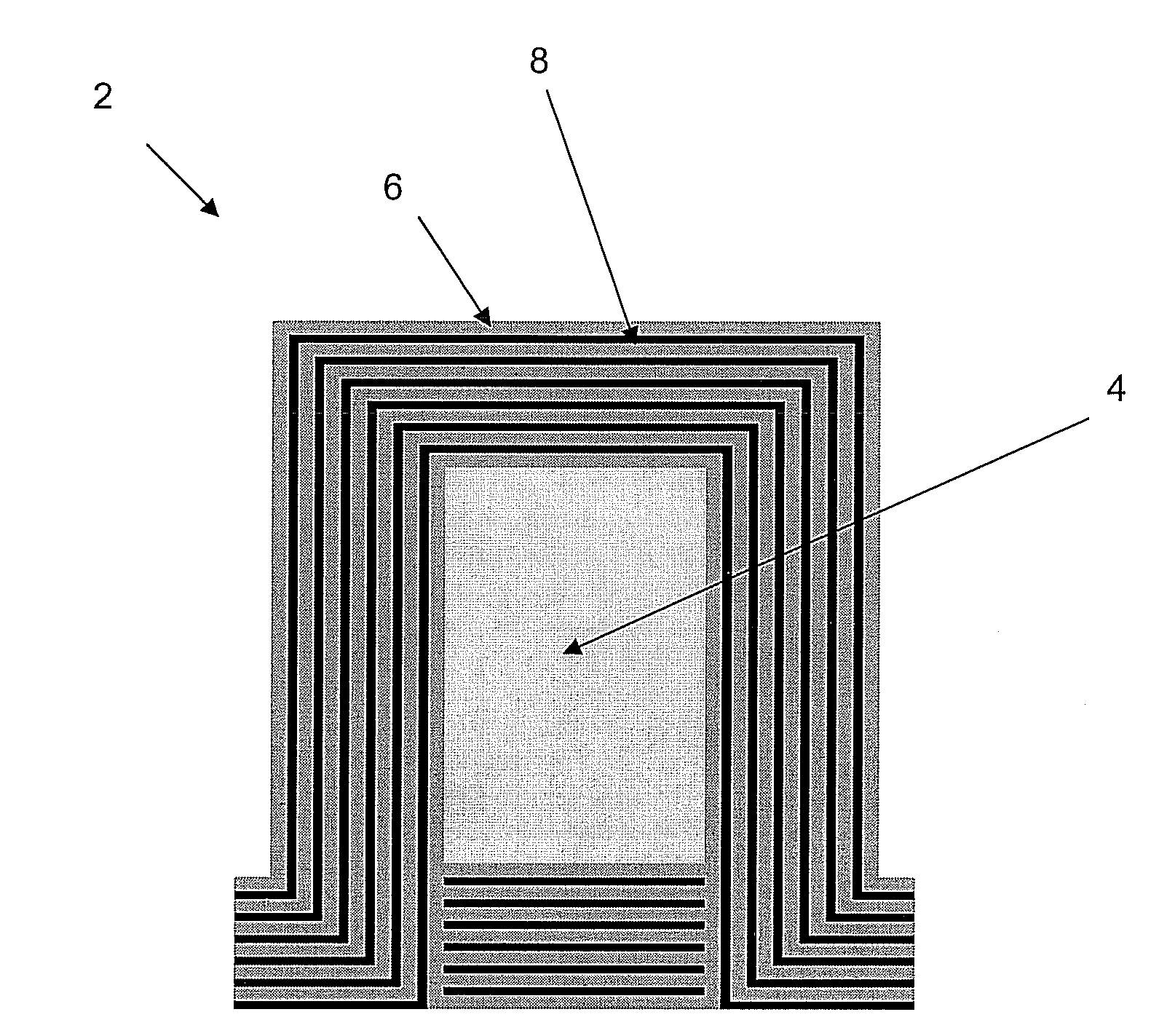
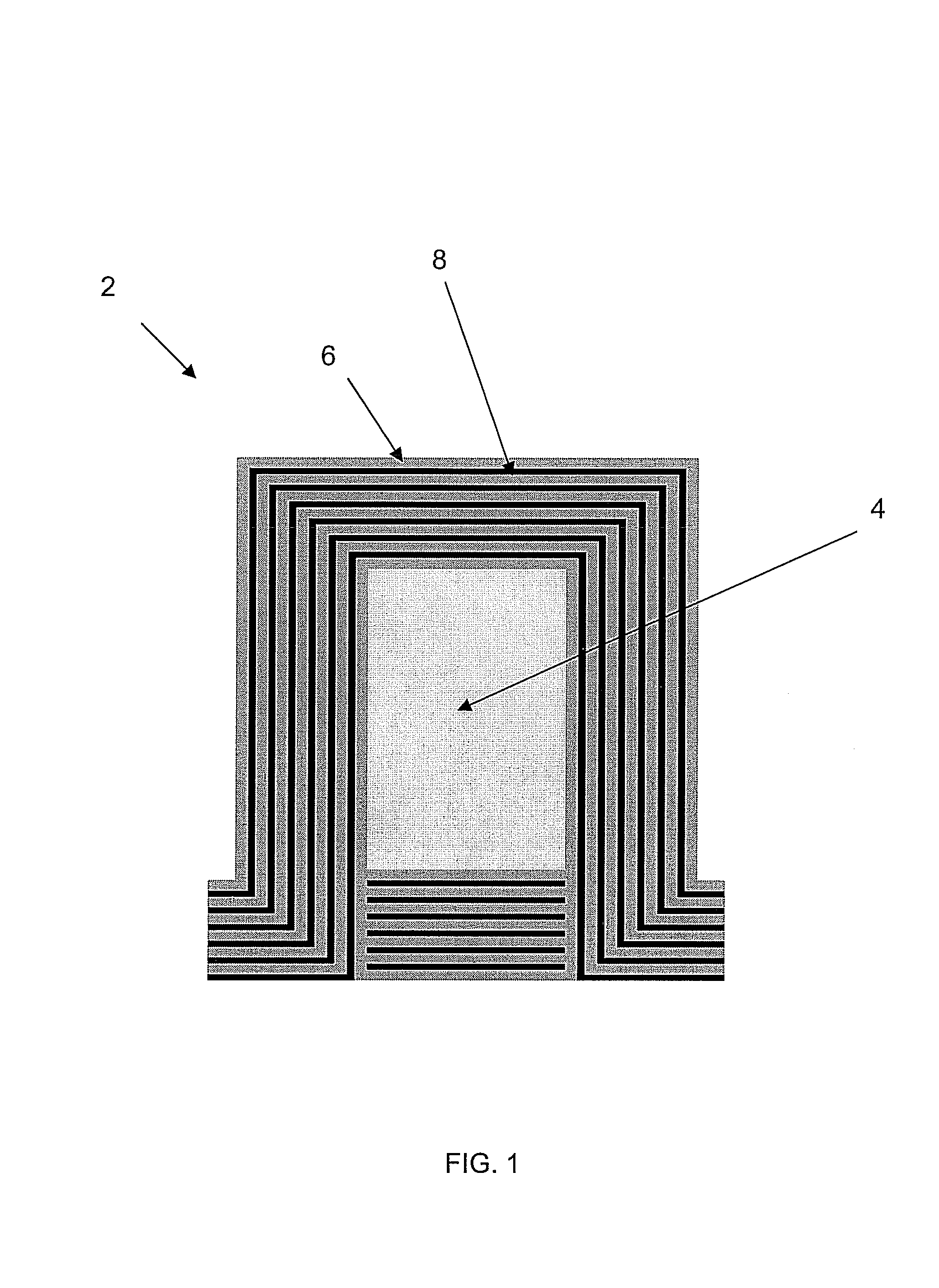
[0014]An on-chip silicon-based Photonic Crystal (PC) cladded waveguide is designed with low refractive index material for the core, and stratified high index contrast dielectric layers as the cladding. Due to the high index contrast of these materials with each other, they have a large photonic band gap, and may act as omnidirectional reflectors, which means light of all incident angles and polarizations is reflected within a range of wavelengths (e.g., near 1550 nm). In contrast with an index-guided waveguide, it is possible to confine light to a low index core (possibly air). The high index contrast allows the cladding thickness to be less than 2 microns, which is much thinner than the conventional silica optical bench waveguide. This structure can also be used to efficiently transmit light about bends much tighter than found in low index contrast index-guided waveguides.
[0015]An on-chip PC cladded waveguide configuration 2 is illustrated in FIG. 1. The inventive on-chip PC wavegu...
PUM
 Abstract
Description
Claims
Application Information
 - R&D Engineer
- R&D Manager
- IP Professional
- Industry Leading Data Capabilities
- Powerful AI technology
- Patent DNA Extraction
Browse by: Latest US Patents, China's latest patents, Technical Efficacy Thesaurus, Application Domain, Technology Topic.
© 2024 PatSnap. All rights reserved.Legal|Privacy policy|Modern Slavery Act Transparency Statement|Sitemap