Antenna using a photonic bandgap structure

a bandgap structure and microstrip technology, applied in the direction of antenna earthings, substantially flat resonant elements, resonant antennas, etc., can solve the problems of large patch size, narrow bandwidth of microstrip patch antennas, and often restrictive design requirements for antennas. the effect of low loss

Inactive Publication Date: 2009-04-21
UNITED STATES OF AMERICA
View PDF13 Cites 44 Cited by
  • Summary
  • Abstract
  • Description
  • Claims
  • Application Information

AI Technical Summary

Benefits of technology

[0021]An advantage of the present invention is the possibility of providing a low loss microstrip antenna that utilizes a high dielectric substrate (∈r approximately equal to 10 or greater) such as duroid, ceramic, or the like.
[0022]These and other objects, features, and advantages of the present invention will become apparent from the drawings, the descriptions given herein, and the appended claims. However, it will be understood that above listed objects and advantages of the invention are intended only as an aid in understanding certain aspects of the invention, are not intended to limit the invention in any way, and do not form a comprehensive or exclusive list of objects, features, and advantages.
[0023]Accordingly, the present invention provides a method for making a microstrip patch antenna. The method may comprise steps such as, for instance, utilizing dielectric material to form a multiband photonic bandgap structure for use as microstrip patch antenna substrate and forming one or more metallic strips on an upper surface of the microstrip patch antenna substrate to act as radiating elements. Other steps may comprise forming a groundplane on a lower surface of the microstrip patch antenna substrate. The method may further comprise utilizing dielectric material with a dielectric constant greater than or equal to 10.
[0024]The method may or may not further comprise integrating a metallic pattern into the groundplane. If used, the metallic pattern may be of various shapes such as a periodic double ring pattern, such as a periodic double ring circle pattern. Other steps may comprise f

Problems solved by technology

Because such antennas have a very low profile and are mechanically rugged, they are often mounted on exposed exterior surfaces of aircraft and spacecraft, and surfaces such as the periscope of a submarine.
In a submarine environment, antenna size is often among the most restrictive of the design requirements.
One disadvantage of microstrip patch antennas is that for lower frequencies a relatively large patch size is required.
Another disa

Method used


Image

  • Antenna using a photonic bandgap structure
  • Antenna using a photonic bandgap structure

Examples


Embodiment Construction

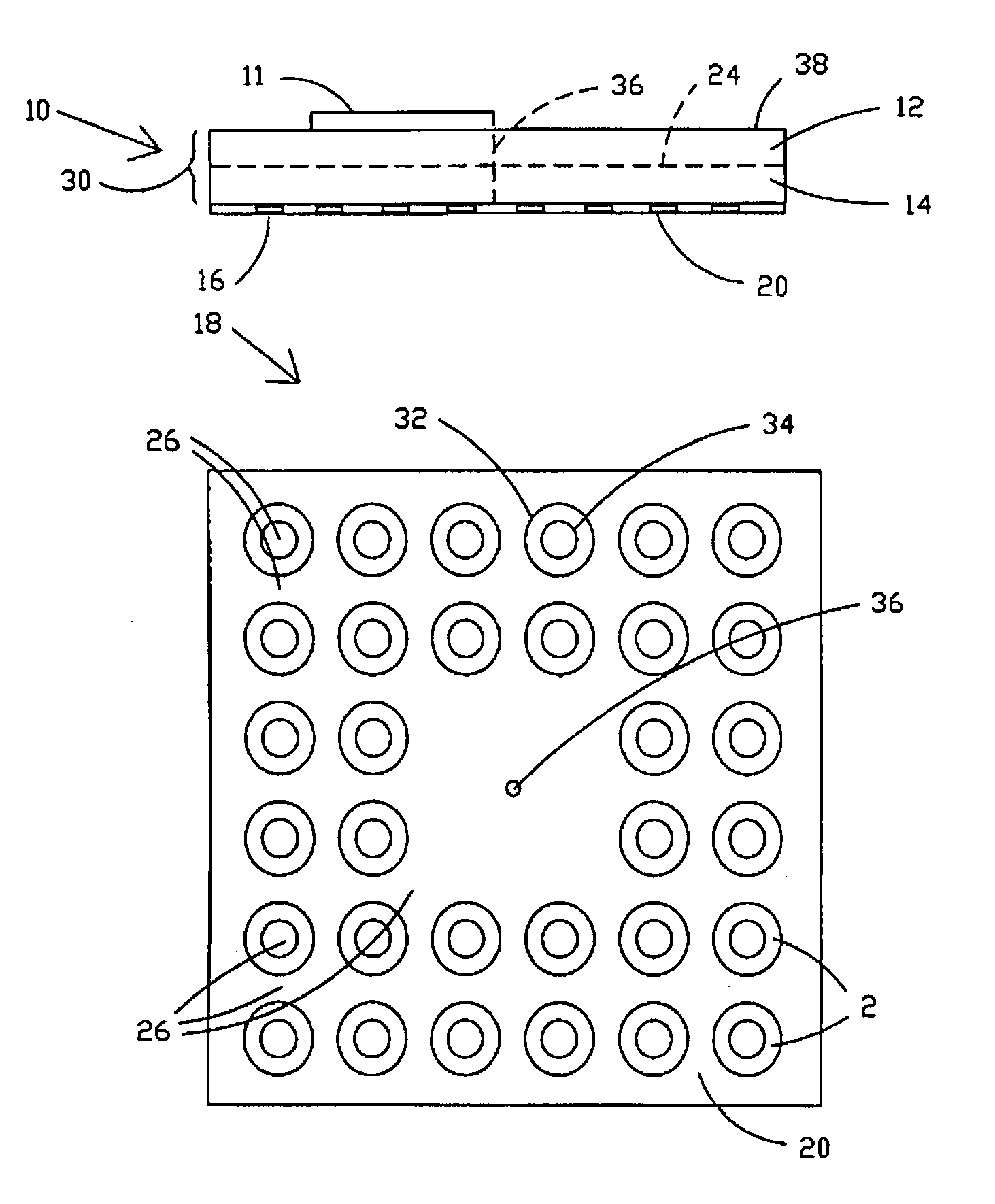
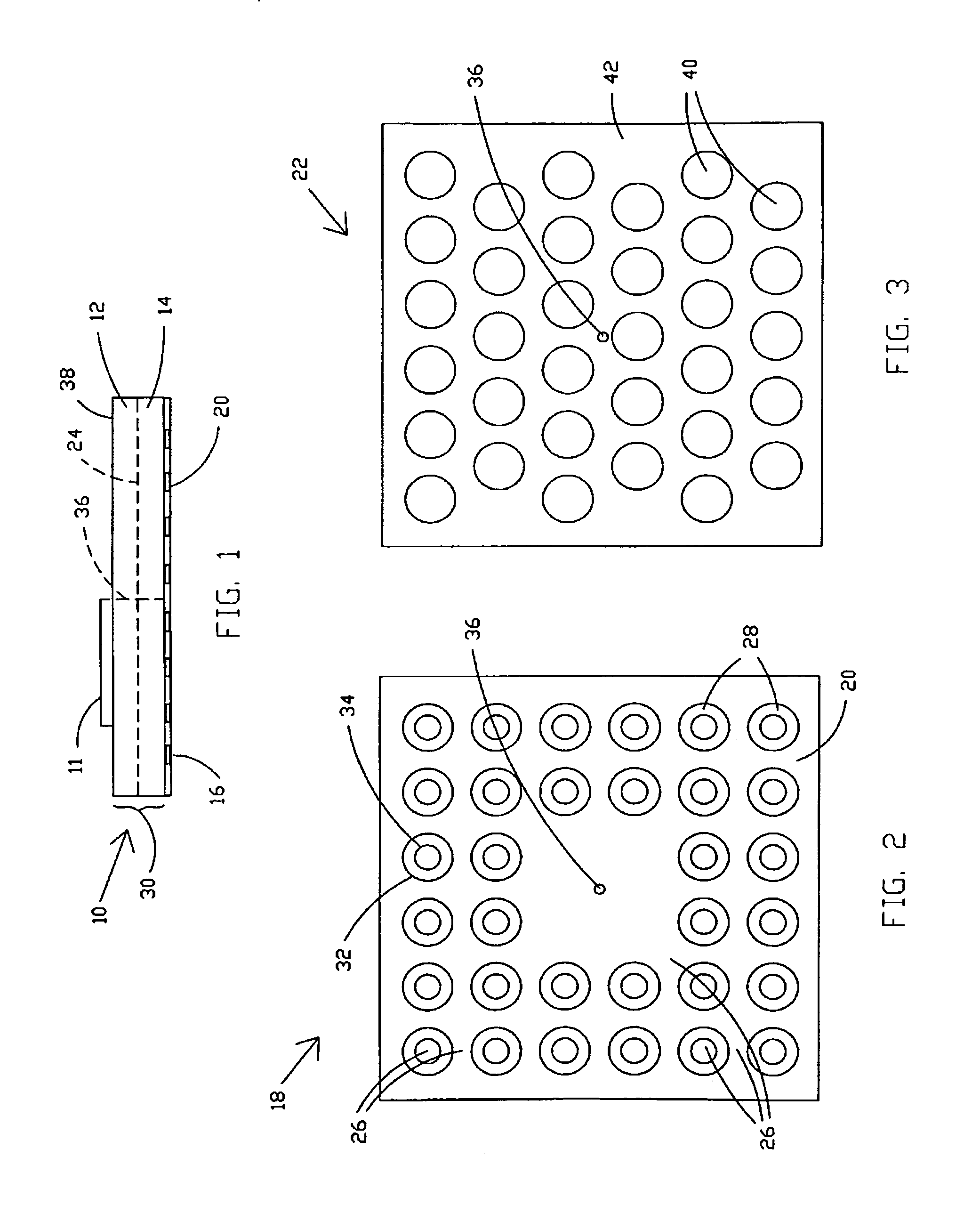
[0031]Antenna gain is directly proportional to antenna size compared to the wavelength. One way to reduce the size of a microstrip patch antenna is to use a high dielectric material as the substrate. This changes the wavelength thus reducing the resonant length of the antenna. However, the higher the dielectric constant, the more energy is passed into the substrate rather than radiated, thus reducing the efficiency of the antenna.

[0032]As discussed hereinbefore, it has been found that a photonic bandgap structure can reduce the energy in the substrate. Photonic bandgap structures introduce periodic “defects” into the substrate much like a Bragg grating or crystal lattice introduces stop bands. Photonic bandgap structures are periodic dielectric structures that have a physical gap that is a bandgap that prevents propagation of electromagnetic waves of a particular frequency or wavelength within the bandgap. As used herein, a multiband photonic bandgap structure prevents propagation o...


PUM


Abstract

A microstrip patch antenna utilizes a microstrip patch antenna substrate formed of photonic bandgap material. One or more periodic patterns may be used therewith to produce multiple bandgaps into the photonic bandgap material. The periodic patterns may be produced by introducing periodic defects into the dielectric material substrate with drilled holes, slots, shorted vias, blind vias, buried vias, and/or plated or unplated patterns, such as plated patterns on the groundplane or on internally positioned surfaces, or on the surface adjacent the radiating elements. One or more radiating elements are used on an upper surface of said microstrip patch antenna substrate, and a groundplane is formed on a lower surface of said microstrip patch antenna substrate.

Description

STATEMENT OF GOVERNMENT INTEREST[0001]The invention described herein may be manufactured and used by or for the Government of the United States of America for governmental purposes without the payment of any royalties thereon or therefore.BACKGROUND OF THE INVENTION[0002](1) Field of the Invention[0003]The present invention relates generally to microstrip patch antennas and, more particularly, to a microstrip patch antenna with a multiband photonic bandgap structure.[0004](2) Description of the Prior Art[0005]Microstrip patch antennas are very well known.[0006]Microstrip patch antennas consist of thin, flat, printed circuit board antennas. Microstrip patch antennas are relatively inexpensive and easy to manufacture. The radiating elements of the antenna are conducting strips or patches printed on the upper surface of a dielectric substrate that is backed by a conducting ground plate or ground plane. Because such antennas have a very low profile and are mechanically rugged, they are ...

Claims


Application Information

Patent Timeline
IPC IPC(8): H01Q1/38
CPCH01Q1/28H01Q1/32H01Q1/34H01Q9/0407H01Q15/006
Inventor LACOMB, JULIE ANNE
Owner UNITED STATES OF AMERICA
Why Eureka
Try Eureka