Printing antenna with baseplate integrated waveguide feeder

A substrate-integrated waveguide and waveguide feeding technology, applied in the field of antennas and feeding, can solve the problem that there are not many types of antennas, and achieve the effects of improving cross-polarization and bandwidth performance, simple and convenient sealing, economical, and high precision

Active Publication Date: 2011-02-16
南京易太可通信技术有限公司
View PDF0 Cites 129 Cited by
  • Summary
  • Abstract
  • Description
  • Claims
  • Application Information

AI Technical Summary

Problems solved by technology

While maintaining the advantages of high power and low loss of traditional waveguides, SIW technology also retains the advantages of general planar printed transmission lines, such as easy integration, light weight, easy processing, and easy sealing. However, there are not many types of antennas suitable for SIW feeding.

Method used


Image

  • Printing antenna with baseplate integrated waveguide feeder
  • Printing antenna with baseplate integrated waveguide feeder
  • Printing antenna with baseplate integrated waveguide feeder

Examples


Embodiment 1

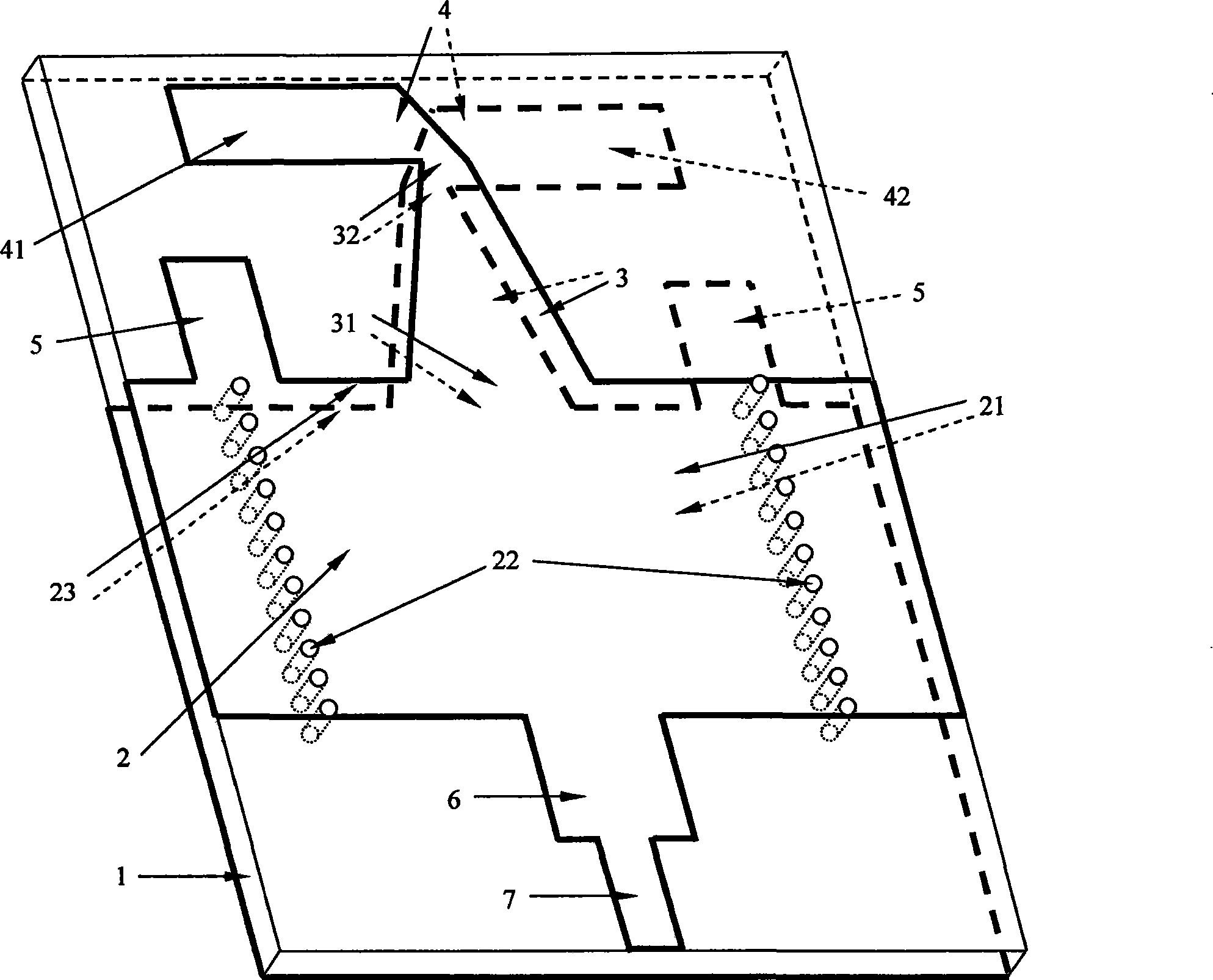
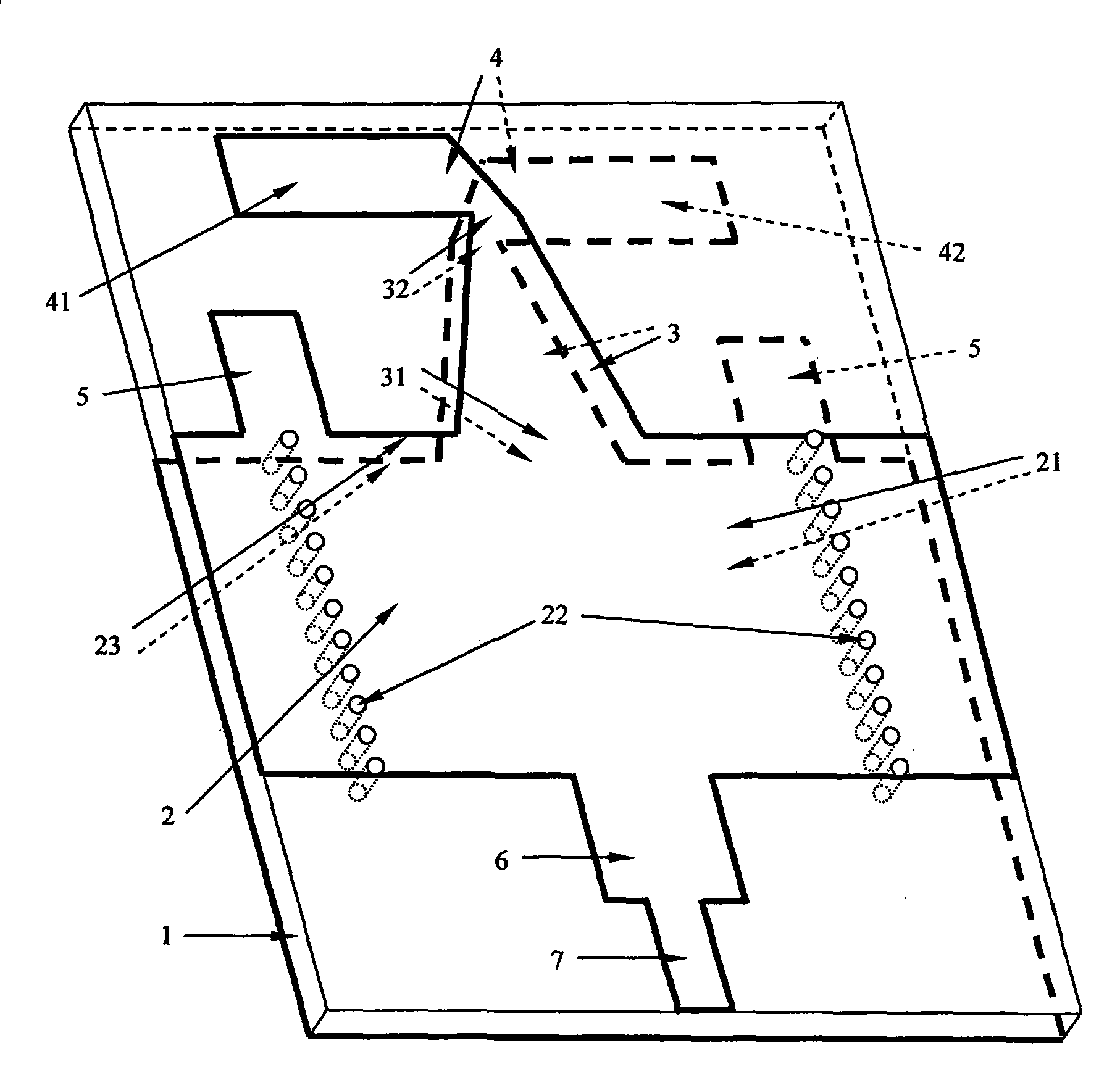
[0018] Embodiment 1 A substrate-integrated waveguide-fed printed antenna with a metal reflector.

[0019] Antenna structure such as figure 2 All dimensions shown are in mm. The size of the metal reflector is 150×150×4 (L×W×H), and a 43×1 slot is opened on the reflector to let the dielectric substrate with the substrate integrated waveguide and the printed antenna pass through. The size of the substrate in this embodiment is 43×44×1. One side of the reflector is the antenna radiating outward, and the other side is the SIW and the transition switch connected with the circuit. The gap is located at the SIW, so that the purpose of sealing and isolation can be achieved, and the short circuit of the radio frequency signal will not be caused because the gap on the metal reflector is connected to the metal on the upper and lower sides of the substrate.

Embodiment 2

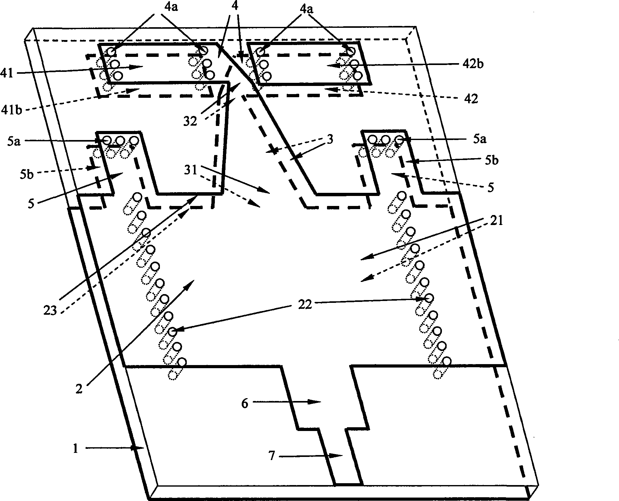
[0020] Embodiment 2 A printed antenna array fed by a waveguide is integrated into a substrate that realizes sealing connection with a circuit shielding box.

[0021] An antenna array structure in which the printed antenna fed by the substrate integrated waveguide is sealed and connected to the circuit inside the circuit shielding box through the gap on the reflector and the shielding box wall. An example is an 8×8 array, and each antenna board is processed with 8 arranged horizontally such as figure 1 or figure 2 The substrate-integrated waveguide-fed printed antenna unit with the structure shown (used in the schematic diagram for the convenience of drawing figure 1 Structure representation), each unit is connected to the corresponding circuit inside the circuit box by the SIW section through the gap on the reflector and the circuit box shell, and there are 8 layers of such circuit boxes and antenna boards arranged vertically to form an 8×8 array. Since the gap of each laye...


PUM


Abstract

A chip integrated waveguide feeding print antenna is composed by a chip with its two metal sides being transfixed with metal through holes in array. The two metal sides are in axial symmetry. There is an intergrading section to one side of the waveguide centerline on two surface of the chip linking with transmission line. To the outer end of the intergrading section links a vibrator antenna. To the opposite side of the intergrading section on the waveguide links a micro-strip intergrading commutator linking with micro-strip transmission line.

Description

technical field [0001] The invention relates to an antenna and feeding technology applied in the fields of wireless communication, electronic reconnaissance and countermeasures, and radar. The application where the antenna feeder needs to be plane integrated and sealed with the system. Background technique [0002] Most of the coaxial lines, rectangular waveguides and antenna structures suitable for these transmission lines are traditional three-dimensional structures. They have the advantages of high power capacity and low loss, but are expensive to process and unsuitable for integration with modern planar circuits. In order to meet the requirements of system integration and equipment lightweight, a variety of antenna and feeder technologies suitable for planar printing processes have been proposed, including microstrip lines, slot lines, coplanar waveguides, etc., and various antennas suitable for these transmission lines. Such as various microstrip antennas and printed ...

Claims


Application Information

Patent Timeline
Patent Type & Authority Patents(China)
IPC IPC(8): H01Q1/38H01Q13/08
Inventor 洪伟蒯振起余晨陈继新田玲严蘋蘋
Owner 南京易太可通信技术有限公司
Why Eureka
Try Eureka