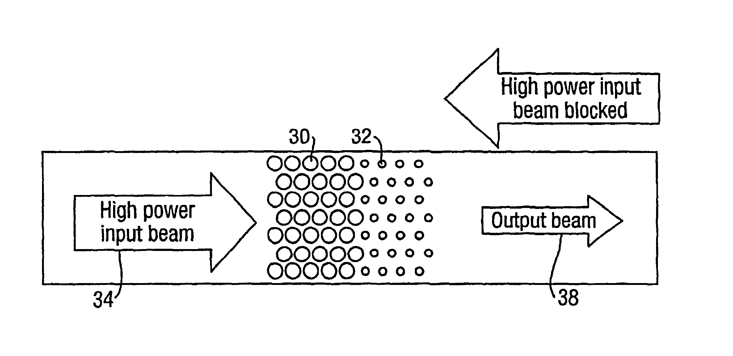
Optical device

a technology of optical devices and optical components, applied in the field of optical devices, can solve the problem that devices are not readily integrated into the circuit arrangement of other optical devices, and achieve the effect of non-linear

Inactive Publication Date: 2005-05-03
NANOGAN
View PDF24 Cites 48 Cited by
  • Summary
  • Abstract
  • Description
  • Claims
  • Application Information

AI Technical Summary

Benefits of technology

[0024]wherein the structure includes a material having first regions of a first refractive index spaced from one another by a second region or regions of a second refractive index in order to provide a crystal or quasicrystal structure exhibiting a photonic band gap, wherein the structure modifies the properties of the material to induce a signifi...

Problems solved by technology

Furthermore, by virtue of their structure, these devices are not ...

Method used


Image

  • Optical device
  • Optical device
  • Optical device

Examples


first embodiment

[0079 of the Invention

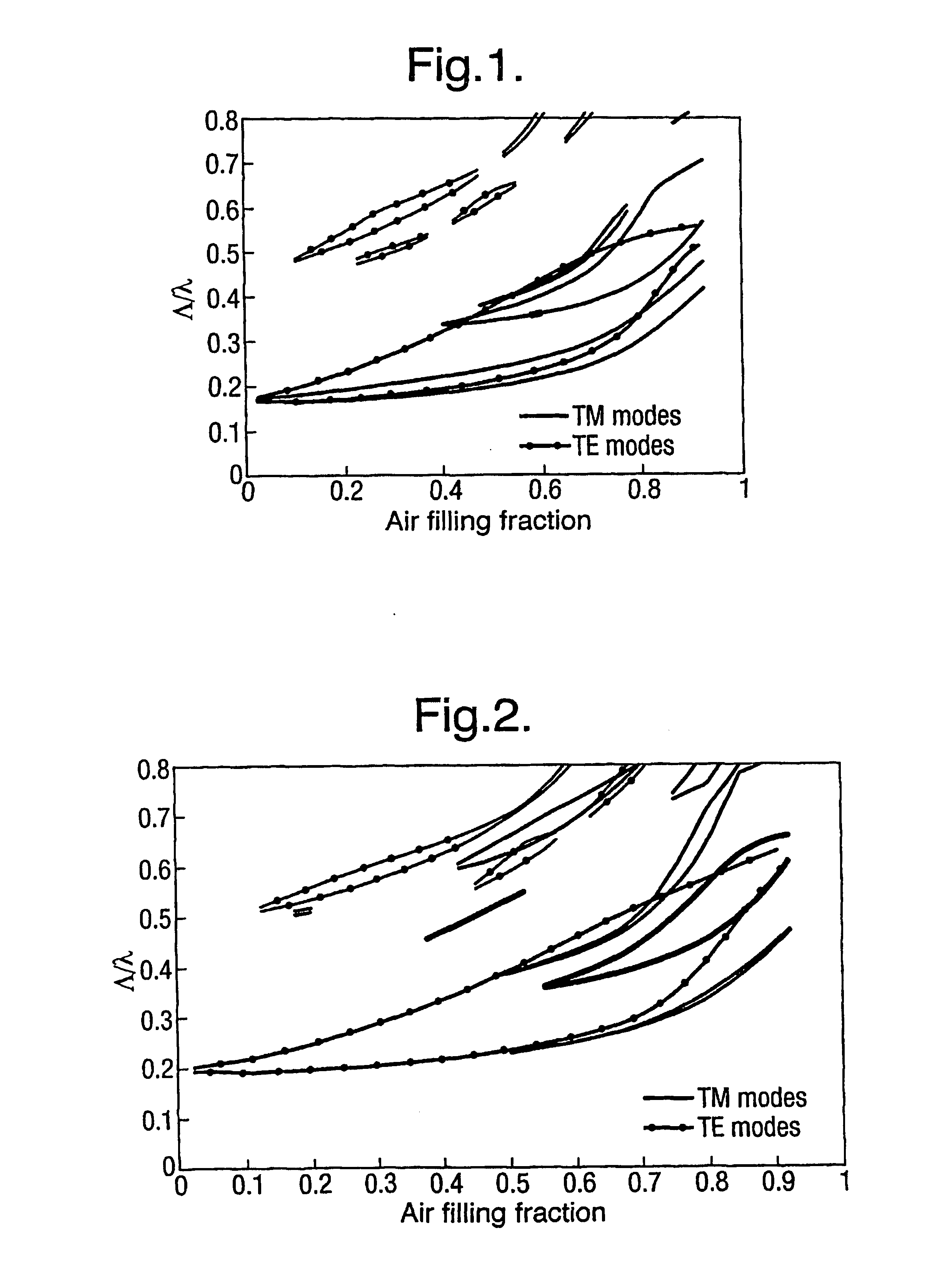
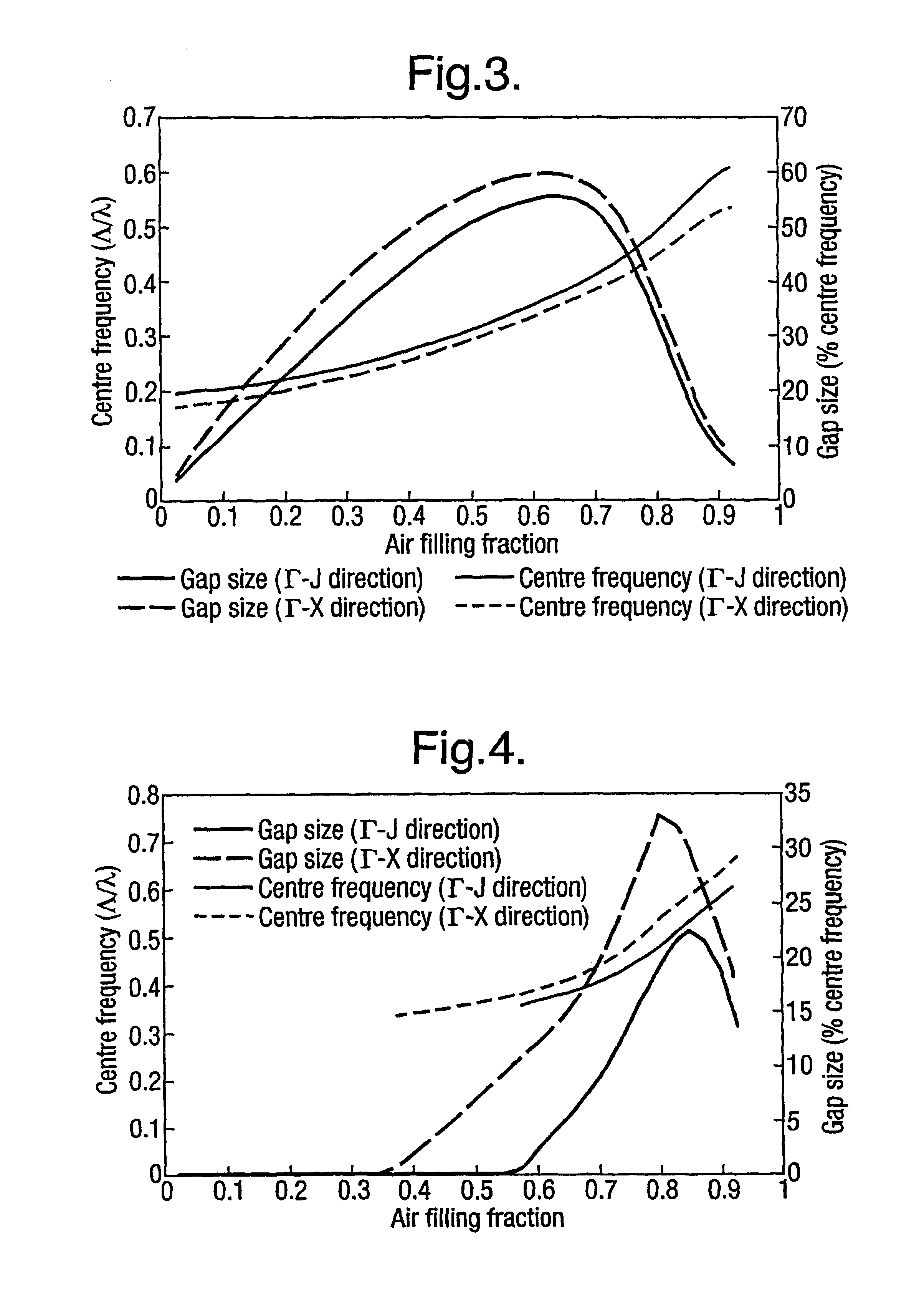
[0080]For many applications involving the use of photonic crystals it is desirable to acquire complete and absolute photonic bandgaps. In the case of such photonic band gap structures, the wave propagation is forbidden for any direction of propagation, and independent of the polarisation state. This provides a preferred photonic band gap structure for the use in applications such as the inhibition of spontaneous emission and polarisation independent devices. Periodic triangular and hexagonal lattice structures can support complete photonic bandgaps in two and three dimensions. However, as shown in FIGS. 9-14, complete and absolute photonic band gaps (CAPBGs) have only been achieved in very high dielectric constant materials like GaAs (ε=13.6) using hexagonal or triangular lattice structures. The frequency range of the bandgaps formed by such a structure is also highly dependent upon the direction of wave propagation, hence the structure is not suitable for all ...


PUM


Abstract

In order to create an optical device with a photonic band gap extending in two dimensions and with very uniform properties in any direction and for any polarisation state, to within 1%, air holes are etched within a substrate of low refractive index material such silicon oxynitride or silica glass. The ratio of air hole area to the remainder of the substrate is low, being less than 35%. The air holes define a quasicrystal structure, having twelve fold symmetry, being based on a square-triangle system. In another development, an etched substrate with a regular crystal structure or quasicrystal structure exhibits a non-linear refractive index. Two adjacent areas in such a substrate have different lattice properties, or have defects in the lattices, to create a unidirectional transmission path (diode action). A further beam of light may be used to modulate the transmission path by reason of the non-linear refractive index.

Description

[0001]This application is the US national phase of international application PCT / GB01 / 01588 filed 06 Apr. 2001, which designated the US.[0002]This invention relates to optical devices and, in particular, to optical devices incorporating structures exhibiting a photonic band gap.[0003]In our prior application WO 98 / 53351, there is described a method of controlling the propagation characteristics of radiation in wave guides by means of photonic band gaps. Such devices may be formed by etching a substance which supports propagation of radiation at a wavelength of interest, for example visible radiation. This radiation may be visible radiation or other forms of electromagnetic radiation such as ultra-violet, infra-red and terahertz radiation. In this specification, the term “optical radiation” includes such other forms of radiation.[0004]U.S. Pat. No. 5,784,400 discloses an optical device incorporating a resonant cavity including a planar two-dimensional periodic dielectric structure wh...

Claims


Application Information

Patent Timeline
IPC IPC(8): C30B33/00G02B6/122G02B6/12G02B1/02G02F1/31G02F1/35
CPCB82Y20/00C30B33/00G02B6/1225C30B29/60G02B6/12
Inventor BAUMBERG, JEREMY J.CHARLTON, MARTIN D. B.NETTI, MARIA C.PARKER, GREGORY J.ZOOROB, MAJD E.
Owner NANOGAN
Why Eureka
Try Eureka