Photonic crystal devices including gain material and methods for using the same

a technology of gain material and photonic crystal, which is applied in the field of photonic crystals, can solve the problems that the significant amount of electromagnetic radiation generated by gain material in known light-emitting photonic crystal devices is not effectively coupled to the waveguid

Active Publication Date: 2007-07-26
HEWLETT-PACKARD ENTERPRISE DEV LP
View PDF15 Cites 48 Cited by
  • Summary
  • Abstract
  • Description
  • Claims
  • Application Information

AI Technical Summary

Benefits of technology

[0013] While the specification concludes with claims particularly pointing out and distinctly claiming that which is regarded as the present invention, the advantages of this invention can be more readily ascertained from the following description of the invention when read in conjunction with the accompanying drawings in which:

Problems solved by technology

However, a significant quantity of electromagnetic radiation generated by gain material in known light-emitting photonic crystal devices is not effectively coupled to the waveguide.

Method used


Image

  • Photonic crystal devices including gain material and methods for using the same
  • Photonic crystal devices including gain material and methods for using the same
  • Photonic crystal devices including gain material and methods for using the same

Examples


Embodiment Construction

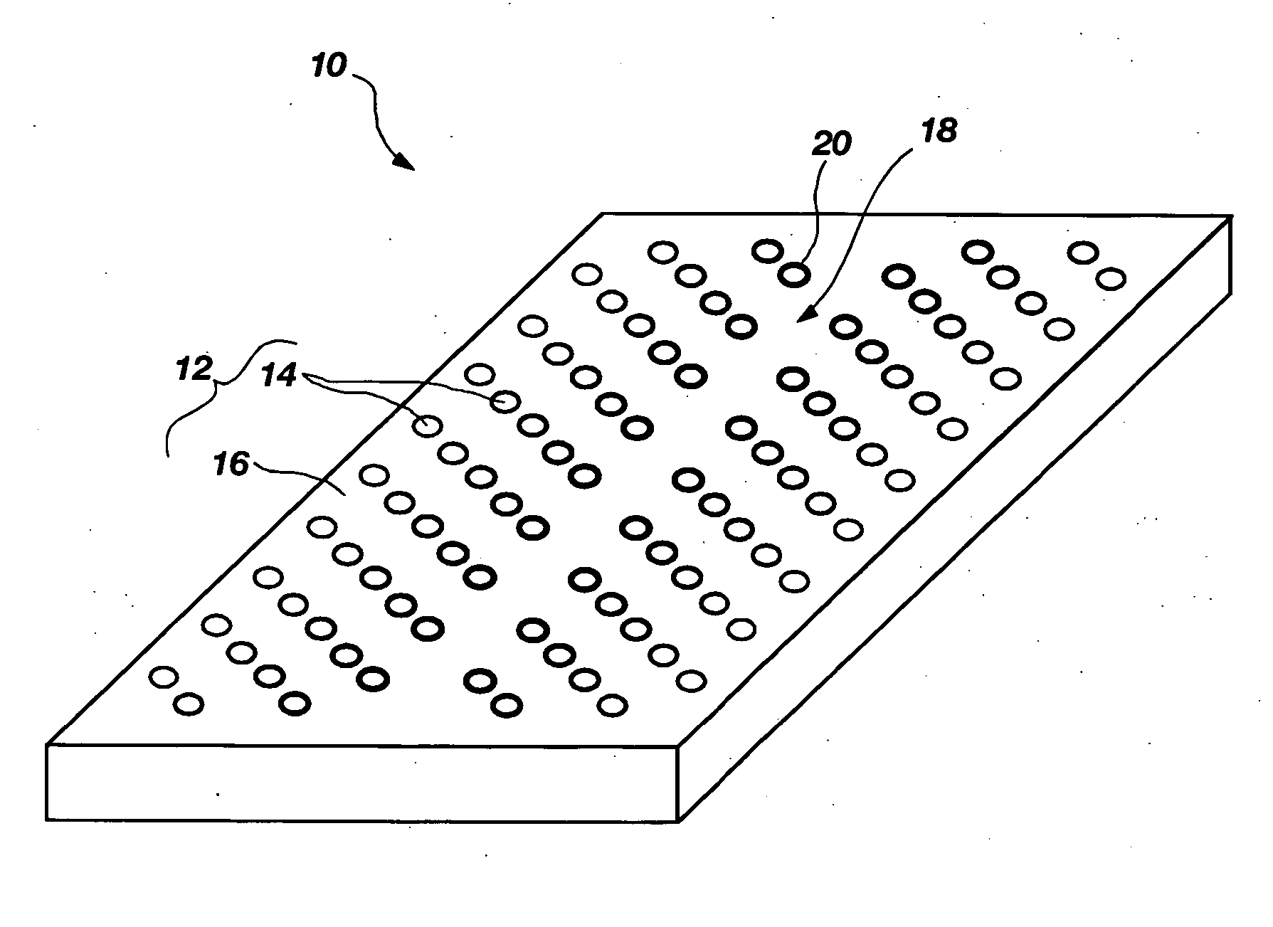
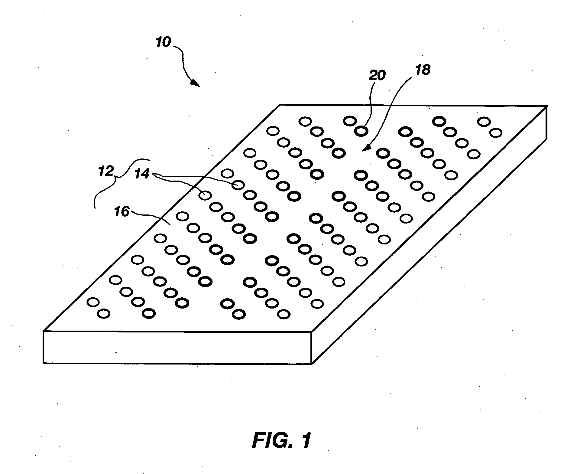
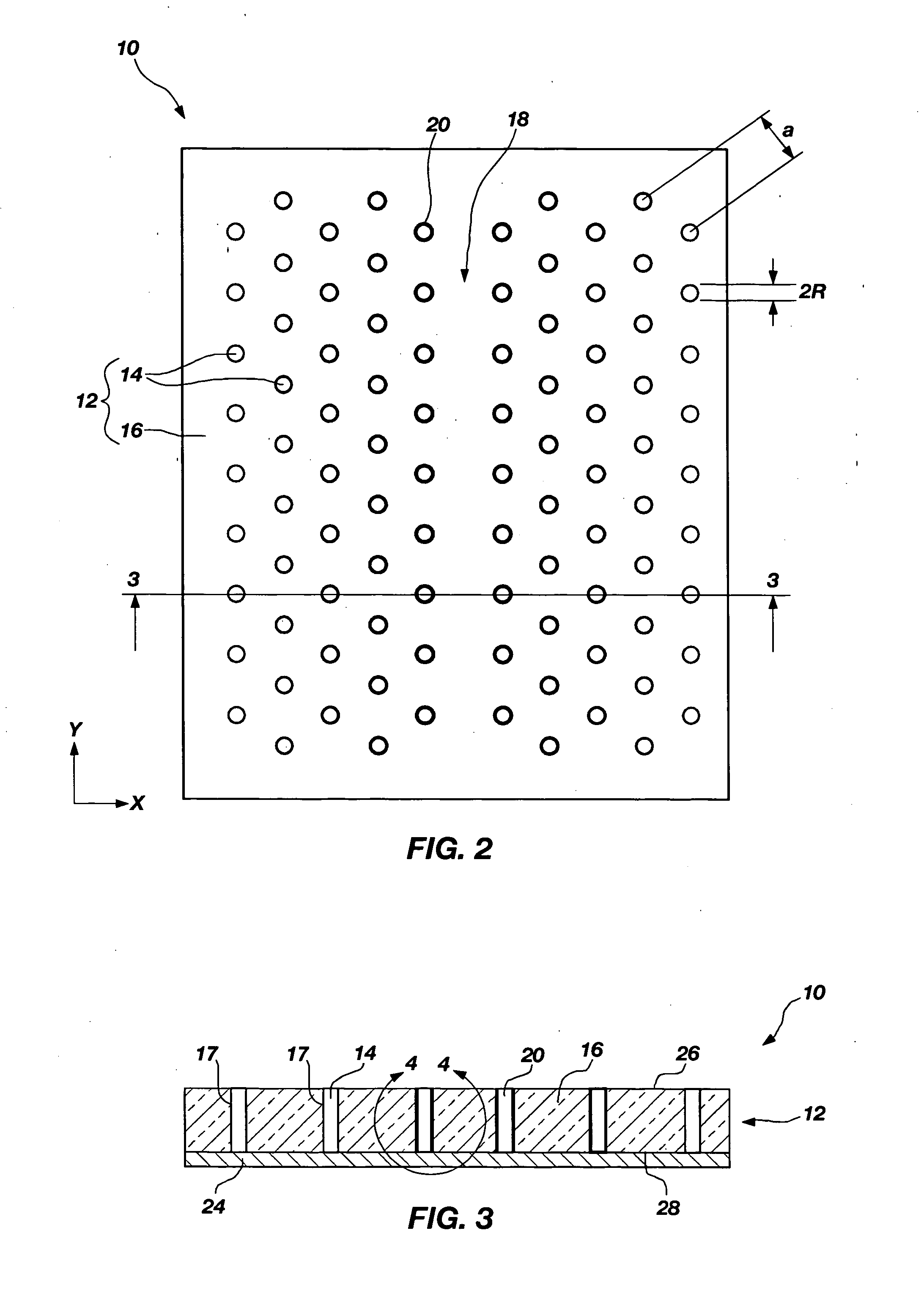
[0027] The illustrations presented herein are not meant to be actual views of any particular photonic crystal device or system, but are merely idealized representations which are employed to describe various aspects of the present invention. Additionally, for ease of discussion, elements common between figures may retain the same numerical designation.

[0028] The term “gain material” as used herein means any material that is capable of emitting electromagnetic radiation upon stimulation. Stimulation may be provided by, for example, electromagnetic radiation (optical pumping) or electrical current (carrier injection).

[0029] The term “nanoparticle” as used herein means a particle of any shape having cross-sectional dimensions of less than about 100 nanometers. Examples of nanoparticles include, but are not limited to, nanodots (including quantum dots), nanowires, nanolines, nanocolumns, and nanospheres.

[0030] The term “waveguide” as used herein means any spatially confined region in...


PUM


Abstract

A device includes a photonic crystal having a plurality of voids disposed in a periodic lattice throughout a dielectric material. Each void is at least partially defined by a surface of the dielectric material. The photonic crystal also includes a waveguide. Gain material is disposed within at least one void located proximate the waveguide. The gain material may emit radiation having a wavelength within a photonic bandgap of the photonic crystal and corresponding to an allowable mode of the waveguide. A method for coupling radiation to a waveguide includes providing a photonic crystal having a plurality of voids disposed in a periodic lattice throughout a dielectric material and a waveguide. Each void is at least partially defined by at least one surface of the dielectric material. Gain material is provided within at least one void located proximate the waveguide and stimulated to emit electromagnetic radiation.

Description

FIELD OF THE INVENTION [0001] The present invention relates to photonic crystals. More particularly, the invention relates to devices that include a photonic crystal having a waveguide and gain material for providing electromagnetic radiation within the waveguide. The invention also relates to methods for coupling electromagnetic radiation to a waveguide. BACKGROUND OF THE INVENTION [0002] Photonic crystals are a new class of man-made materials. They are often referred to as “metamaterials.” Photonic crystals are formed by dispersing a material of one dielectric constant periodically within a matrix having a different dielectric constant. A one-dimensional photonic crystal is a three-dimensional structure that exhibits periodicity in dielectric constant in only one dimension. Bragg mirrors are an example of a one-dimensional photonic crystal. To form a Bragg mirror, alternating thin layers having different dielectric constants and refractive indices are stacked on top of one another...

Claims


Application Information

Patent Timeline
Patent Type & Authority Applications(United States)
IPC IPC(8): G02B6/032G02B6/02
CPCB82Y20/00H01S5/105G02B6/1225H01S5/11
Inventor WANG, SHIH-YUAN
Owner HEWLETT-PACKARD ENTERPRISE DEV LP
Why Eureka
Try Eureka