Timing closure for system on a chip using voltage drop based standard delay formats

a timing analysis and voltage drop technology, applied in the field of timing analysis techniques, can solve the problems of increasing test time, affecting the timing of system on the chip, so as to achieve less pessimistic timing analysis and less on the margins

Active Publication Date: 2008-01-29
TEXAS INSTR INC
View PDF12 Cites 10 Cited by
  • Summary
  • Abstract
  • Description
  • Claims
  • Application Information

AI Technical Summary

Problems solved by technology

This results in considerable voltage drop from periphery to the center of the chip for wire bond designs for both functional (or “mission mode”) and test modes.
These voltage drops are seen to be worse in the case of test modes, as almost all the flops are switching simultaneously.
Such methods however, generally increase test time which adversely impacts the bottom line.
This technique results in extra gates on the die.
Further, voltage drops are not necessarily identical for functional and test modes.
IR drop analysis today is pessimistic, which results in additional margins that increase cycle times for timing closure and potentially increases die size.
Further, today's design flow does not comprehend dynamic voltage drop.

Method used


Image

  • Timing closure for system on a chip using voltage drop based standard delay formats
  • Timing closure for system on a chip using voltage drop based standard delay formats
  • Timing closure for system on a chip using voltage drop based standard delay formats

Examples


Embodiment Construction

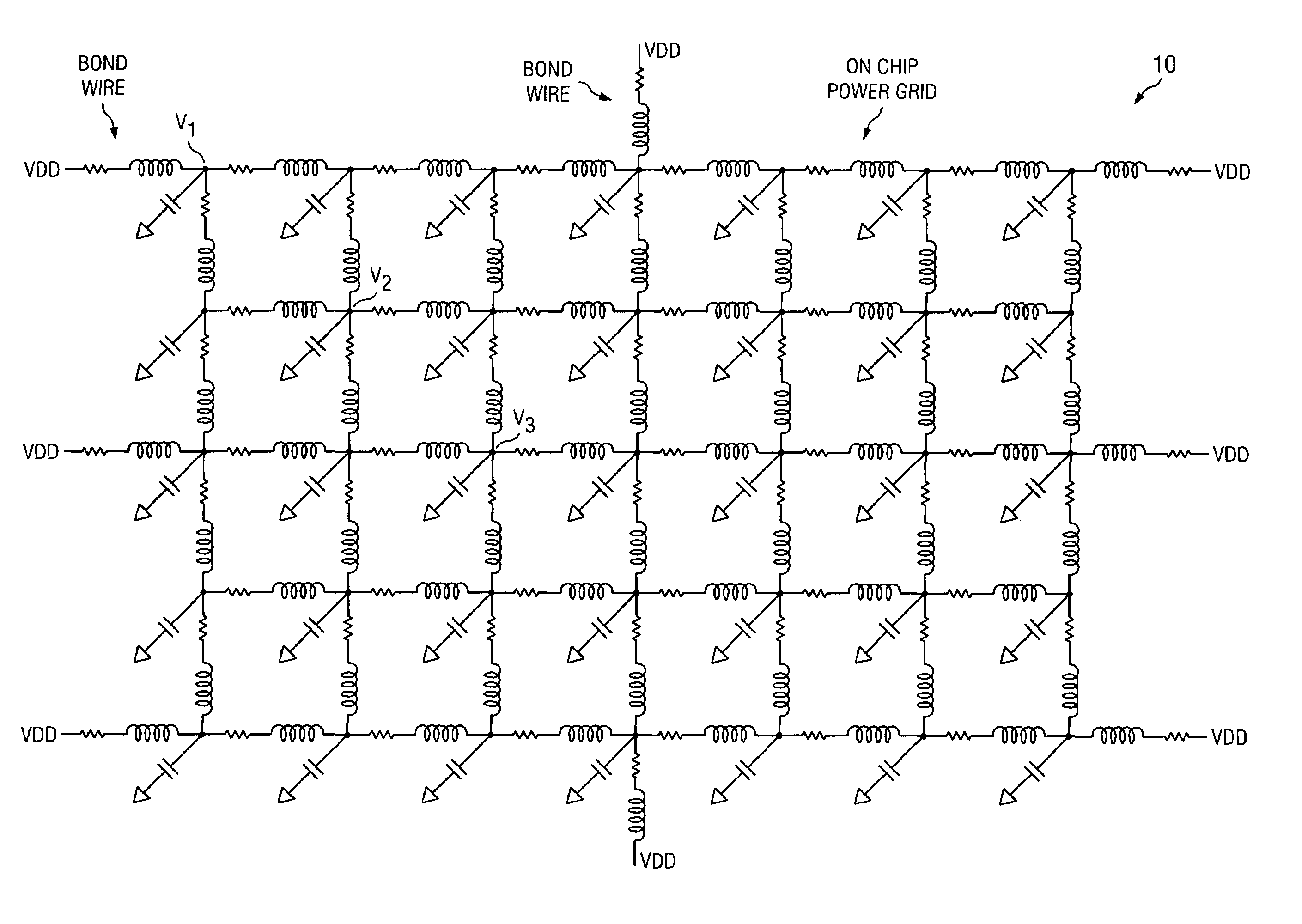
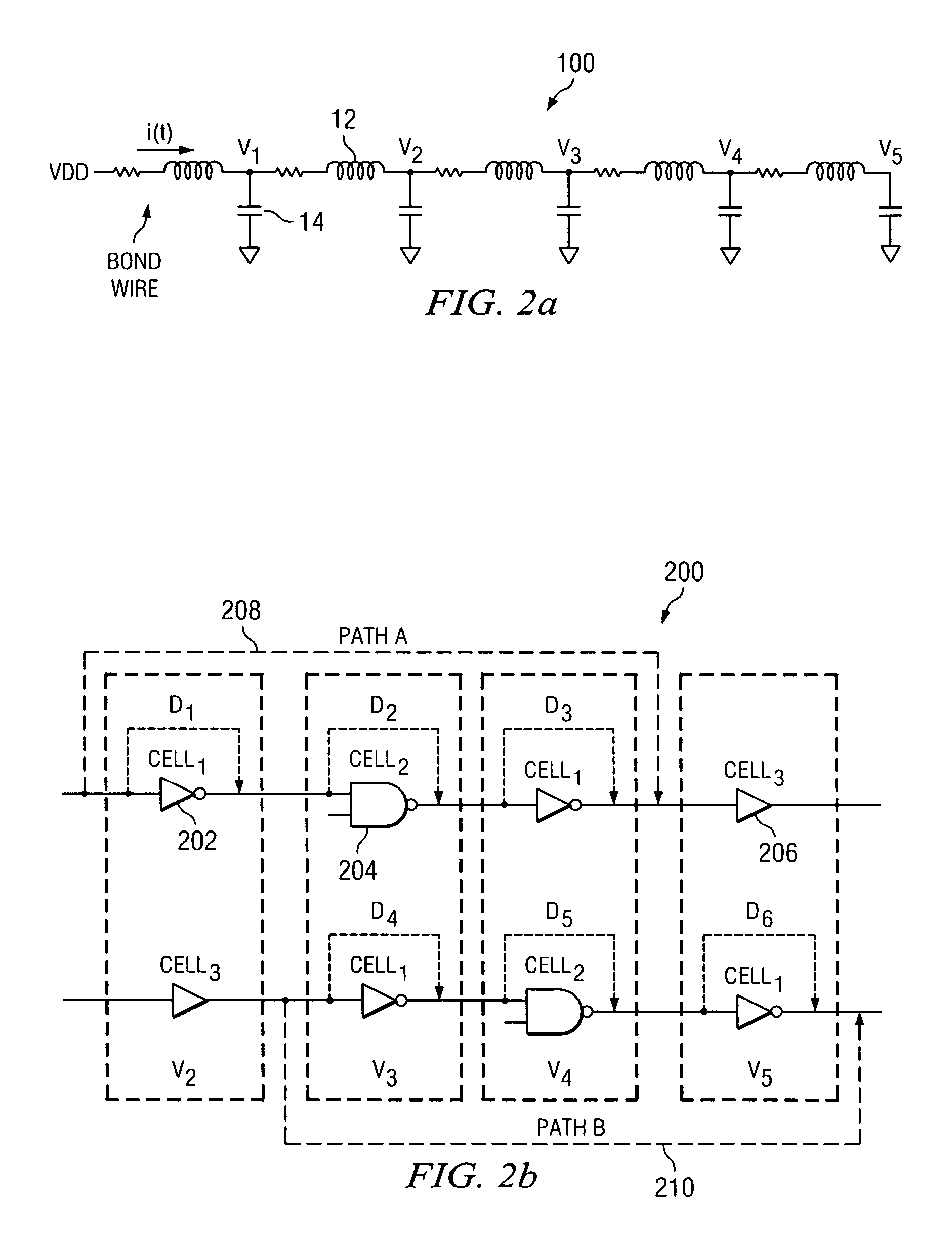
[0019]FIG. 1 is a schematic diagram illustrating a typical power grid model 10 to determine timing closure for SoCs using voltage drop based SDFs; while FIGS. 2a and 2b depict schematic diagrams illustrating one embodiment of an on chip power grid 100 and one embodiment for three different cells instantiated multiple times 200. Assuming that inductors 12 are shorted and that capacitors 14 are open, the power grid 10, 100 can of course, be modeled as resistors only. Such a resistive model implies that voltage drop=IR (under static conditions), and is generally computed based on average current. Comprehending inductance as other than a short implies that voltage drop=i(t)R (static)+Ldi / dt (dynamic). The particular model employed depends upon the mode of operation as well as the frequency of operation. With continued reference now to FIG. 2a, typically VDD>V1>V2>V3>V4>V5 because of voltage drop.

[0020]Moving now to FIG. 2b, consider three different cells 202, 204, 206 (Cell1, Cell2, Cel...


PUM


Abstract

A timing closure analysis associated with SoCs uses voltage drop based standard delay formats (SDFs). Static timing analysis (STA) is implemented using multiple SDFs, one for each mode (ATPG Test, BIST Test, Functional) as contrasted with doing STA with only one worst-case SDF for all modes. The multiple SDFs account for the impact of dynamic voltage drops on delays in addition to static IR drops.

Description

BACKGROUND OF THE INVENTION[0001]1. Field of the Invention[0002]This invention relates generally to timing analysis techniques, and more particularly to a method, of implementing static timing analysis associated with System-on-chips (SoCs).[0003]2. Description of the Prior Art[0004]Today's SoCs consist of several million gates of equivalent logic and memory running at high clock frequencies. This results in considerable voltage drop from periphery to the center of the chip for wire bond designs for both functional (or “mission mode”) and test modes. These voltage drops are seen to be worse in the case of test modes, as almost all the flops are switching simultaneously. Techniques have been devised to minimize voltage drop in the test mode. Such methods however, generally increase test time which adversely impacts the bottom line.[0005]At present, to compensate for voltage drop, designs are built with margins for timing closure. Each static timing analysis (STA) run is typically don...

Claims


Application Information

Patent Timeline
Patent Type & Authority Patents(United States)
IPC IPC(8): G06F19/00G06F9/45
CPCG01R31/31725
Inventor JAIN, ATUL K.PUVVADA, VENUGOPALSAXENA, JAYASHREE
Owner TEXAS INSTR INC
Why Eureka
Try Eureka