
System and method for AC performance tuning by thereshold voltage shifting in tubbed semiconductor technology

a technology of voltage shifting and ac performance, applied in the field of integrated circuit chips, can solve the problems of vt, discarded products or sorted into less-profitable speed bins, and the presence of ac defects in manufactured devices,

Inactive Publication Date: 2002-11-26
IBM CORP
View PDF20 Cites 28 Cited by
  • Summary
  • Abstract
  • Description
  • Claims
  • Application Information

AI Technical Summary

Benefits of technology

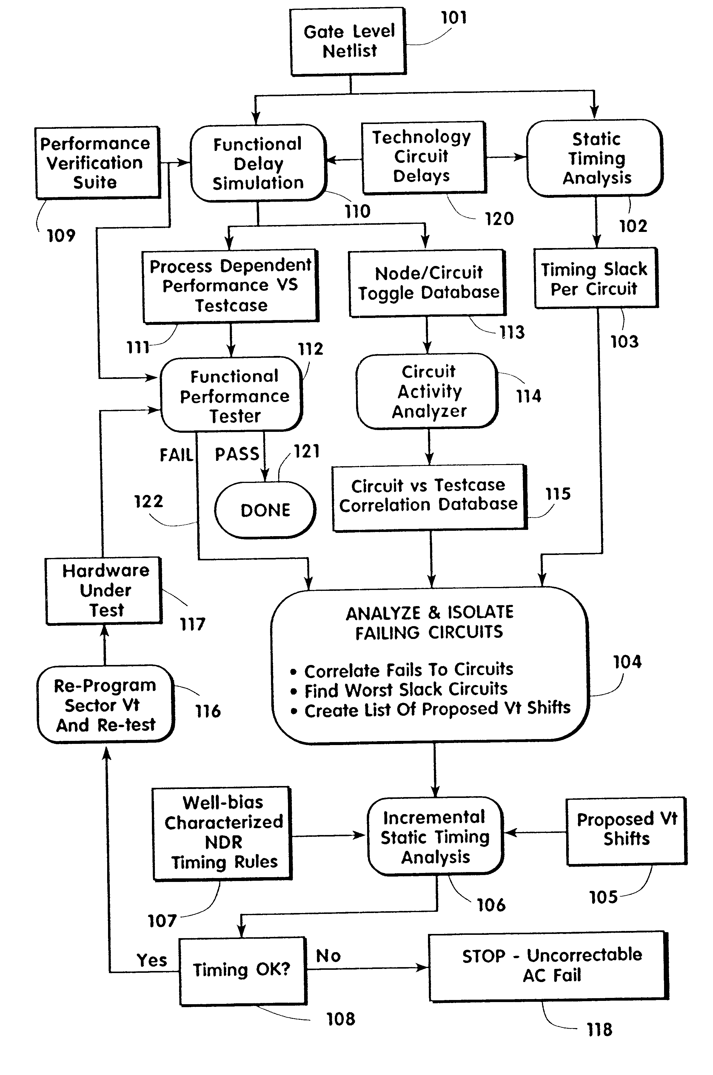
The above and other objects and advantages, which will be apparent to one of skill in the art, are achieved in the present invention which is directed to, in a first aspect, a method for reducing AC test failures during performance testing of an integrated circuit wafer having a plurality of gates, circuits, and bulk well voltages, the method comprising: analyzing each of the plurality of circuits against a plurality of performance verification test cases; identifying failed circuits that do not pass the plurality of performance verification test cases; calculating voltage threshold values for the failed circuits; performing a static timing analysis on the plurality of circuits, substituting the calculated voltage threshold values for the bulk well voltages; programming the integrated circuit wafer to operate at the calculated voltage threshold values that pass the static timing analysis; and, reanalyzing the plurality of circuits having programmed the calculated voltage threshold values against the plurality of performance verification tests.

Problems solved by technology

As the performance targets for integrated circuits increase, the presence of AC defects within the manufactured device is of greater concern due to test cost and yield impacts.
While present test methodologies test for AC defects, products failing these tests are discarded or sorted into less-profitable speed bins.
It is difficult, however, to choose the VT such that the transistor will operate efficiently over a wide range of supply voltages.
Additionally, manufacturing inconsistencies will also cause variations in the threshold voltage among individual transistors.
Several innovative techniques for controlling well bias have been previously disclosed, however, all lack a defined methodology for performing in-situ testing of semiconductors.
Moreover, these prior art techniques have not been built around characterized technology circuit delay timing rules, which allow for safe tailoring of threshold voltages via well bias in order to speed up AC performance without introducing new timing problems such as undesired fast paths.
Although in many cases, the base wafer upon which the FETs without tubs were produced was highly resistive, the isolation between FET regions was not sufficient for independent back biasing of device regions without wells.
In silicon-on-insulator (SOI) technology, n-FETs and p-FETs are both isolated in the locale of device level tubs; however, shallow SOI technologies leave the body of the device floating.
However, there is no analytical mechanism for determining the appropriate bias voltage level and then reanalyzing at this new level for system performance during AC testing.
As indicated by the above-cited prior art, active bulk well voltage control is being used for leakage power control under idle conditions or under program control, in part to enhance product yields, but no methodology or technique currently exists for AC performance tailoring of portions of ASIC devices based on characterized design rule data.
Specifically, active circuits are not directly targeted for appropriate and selective threshold voltage shifting.
Ordinarily, such devices would either be scrapped as out-of-specification where performance sorting was not done, or sorted to slower performance sorts with lower profit margins where performance sorting was practiced.

Method used


Image

  • System and method for AC performance tuning by thereshold voltage shifting in tubbed semiconductor technology
  • System and method for AC performance tuning by thereshold voltage shifting in tubbed semiconductor technology
  • System and method for AC performance tuning by thereshold voltage shifting in tubbed semiconductor technology

Examples


Embodiment Construction

)

In describing the preferred embodiment of the present invention, reference will be made herein to FIGS. 1-4 of the drawings in which like numerals refer to like features of the invention. Features of the invention are not necessarily shown to scale in the drawings.

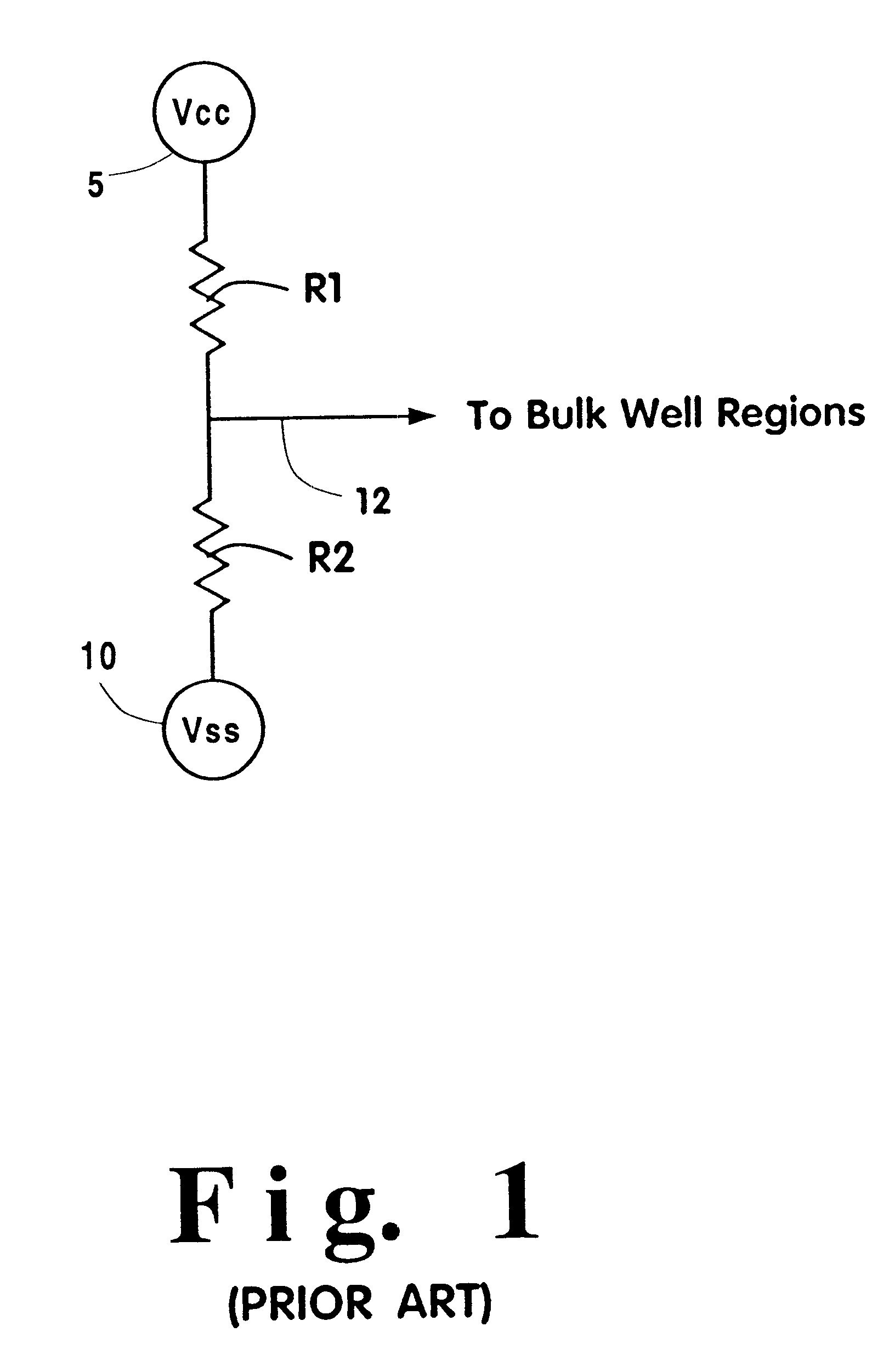
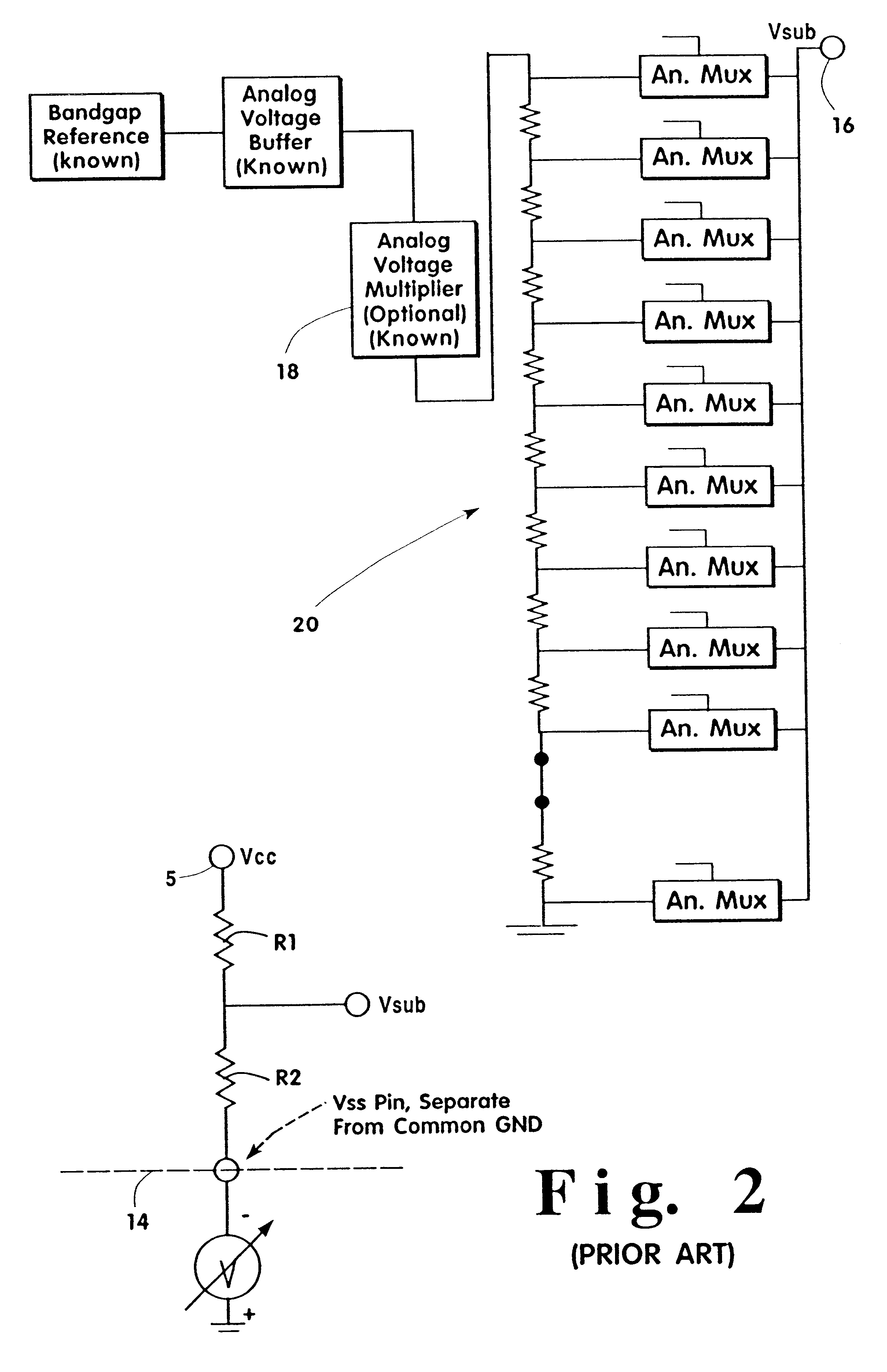
A system and method are described for separating the bulk connections for FETs on the die from the supply rails, testing the die to determine if a shift in the threshold voltage, V.sub.T, of certain devices within the die (as defined by the wells) can remove an AC defect, and tailoring the voltage or voltages applied to the bulk nodes, post-manufacture, such that the integrated circuit meets its performance targets or may be sorted to a more valuable performance level. While the present invention is useful in all FET based integrated circuits, its utility is increased with increases in the number of device wells that may be independently biased, such as in advanced CMOS processes.

In all prior art embodiments for altering ...


PUM


Abstract

A system and method are described for separating the bulk connections for FETs on a semiconductor wafer from the supply rails, testing the wafer to determine if a shift in the threshold voltage, VT, of certain devices within the wafer, as defined by the bulk-wells, can remove an AC defect in the IC circuit, and tailoring the voltage or voltages applied to the bulk nodes, post-manufacture, such that the integrated circuit meets its performance targets or is sorted to a more valuable performance level. The method requires generating a gate level netlist of the IC's circuitry and performing timing calculations on these circuit netlists using static timing analyses, functional delay simulations, circuit activity analyses, and functional performance testing. The failures are then correlated to respective IC circuits, worst case slack circuits are investigated, and proposed changes to the threshold voltages are employed in the hardware.

Description

1. Field of the InventionThis invention relates generally to integrated circuit chips, and more particularly to a system and automated methodology for ac performance tuning of tubbed semiconductor ASIC chips in a timing-safe environment by repairing detected AC defects in the semiconductor die.2. Description of Related ArtAs the performance targets for integrated circuits increase, the presence of AC defects within the manufactured device is of greater concern due to test cost and yield impacts. While present test methodologies test for AC defects, products failing these tests are discarded or sorted into less-profitable speed bins.In order to improve the AC yield characteristics produced by IC devices, a system and method for tailoring device performance post-manufacture is disclosed. The means described allows for tailoring of the bulk voltage supplied to various well structures within the die, thereby altering the effective threshold voltage and AC performance of the devices pres...

Claims


Application Information

Patent Timeline
IPC IPC(8): G01R31/3163G01R31/28
CPCG01R31/2891G01R31/3163
Inventor DEAN, ALVAR A.HAYES, JERRY D.IADANZA, JOSEPH A.KELLER, EMORY D.VENTRONE, SEBASTIAN T.
Owner IBM CORP
Learn More