Semiconductor testing equipment, testing method for semiconductor, fabrication method of semiconductor, and semiconductor memory

a technology of semiconductor testing equipment and fabrication methods, which is applied in the direction of error detection/correction, instruments, computing, etc., can solve the problems of increasing increasing the price of fail memory, and reducing the fabrication yield of memory, so as to reduce the price of semiconductor testing equipment, reduce the failure address memory capacity, and reduce the fabrication yield of high-capacity memory

Inactive Publication Date: 2006-11-14
HITACHI LTD +1
View PDF12 Cites 38 Cited by
  • Summary
  • Abstract
  • Description
  • Claims
  • Application Information

AI Technical Summary

Benefits of technology

[0009]Furthermore, in testing the semiconductor memory, normally, a number of memories are simultaneously tested (e.g., 64 memories per one testing equipment) in order to reduce the costs for test (test cost) and the time for test (test time). Therefore, since the above-mentioned fail memory is required to be increased in capacity similarly to the simultaneous test, the price of the equipment further is increased.
[0020]Furthermore, according to the present invention, the screening inspection and the redundancy processing are performed by the same semiconductor testing equipment, so that the memory capacity for the fail address can be decreased by the result that the reducing of the price of the semiconductor testing equipment and the shortening of the processing time thereof can be realized and, in the end, the low price of the semiconductor memory can be realized.

Problems solved by technology

However, since a ratio of defection generated in one memory chip increases along with an increase in the capacity of the memory to be a test object, a fabrication yield of the memory is decreased due to an increase in the capacity thereof.
For this reason, the price of the fail memory is increased and the price of the semiconductor testing equipment is also increased accordingly.
Therefore, since the above-mentioned fail memory is required to be increased in capacity similarly to the simultaneous test, the price of the equipment further is increased.

Method used


Image

  • Semiconductor testing equipment, testing method for semiconductor, fabrication method of semiconductor, and semiconductor memory
  • Semiconductor testing equipment, testing method for semiconductor, fabrication method of semiconductor, and semiconductor memory
  • Semiconductor testing equipment, testing method for semiconductor, fabrication method of semiconductor, and semiconductor memory

Examples


first embodiment

[0033](First Embodiment)

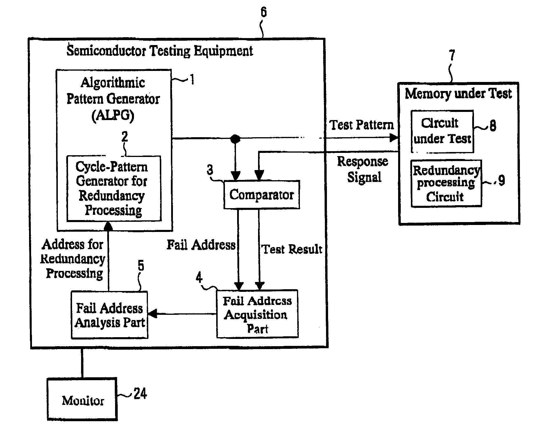
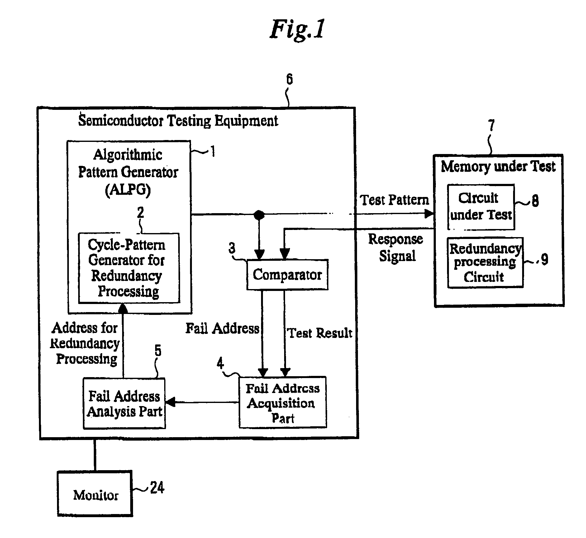
[0034]In the beginning, by using FIG. 1, one example of a structure of one piece of semiconductor testing equipment according to a first Embodiment of the present invention will be described.

[0035]The semiconductor testing equipment 6 according to this embodiment of the present invention comprises: an algorithmic pattern generator 1 (ALPG: Algorithmic Pattern Generator), which generates a test pattern for testing a memory under test 7 and applies the pattern to the memory under test 7; a comparator 3 for making comparison of a response signal from the memory under test 7 and an expected value obtained from the algorithmic pattern generator 1; a fail address acquisition part 4 for storing a fail address in accordance with test results obtained from the comparator 3; a fail address analysis part for calculating an address to be repaired by analyzing the fail address stored in the fail address acquisition part 4, and a cycle-pattern generator for redundancy proc...

second embodiment

[0084](Second Embodiment)

[0085]By using FIG. 10, one structural example of the semiconductor testing equipment according to a second embodiment of the present invention will be described. FIG. 10 shows a structure of the semiconductor testing equipment according to a second embodiment of the present invention.

[0086]The first embodiment has a structure for testing the memories under test 7 one by one, while one piece of semiconductor testing equipment 6a according to the present embodiment has a structure for testing a plurality of memories under test 7 concurrently.

[0087]That is, the semiconductor testing equipment 6a according to the second embodiment comprises one test circuit 22, This test circuit 22 comprises an algorithmic pattern generator 19 a fail address analysis part 5, and a plurality of device controllers 23, wherein the algorithmic pattern generator 1 includes a cycle-pattern generator for redundancy processing 2 and each of the device controllers 23 includes the compar...

third embodiment

[0092](Third Embodiment)

[0093]By using FIG. 11, one structural example of one piece of semiconductor testing equipment according to a third embodiment of the present invention will be described. FIG. 11 shows a structure of the semiconductor testing equipment according to a third embodiment.

[0094]Similarly to the second embodiment, one piece of semiconductor testing equipment 6b according to the present embodiment includes a structure for testing a plurality of memories under test 7 simultaneously and further have a structure in which the test circuits 22a equal to the memories under test 7 in number are mounted.

[0095]That is, this semiconductor testing equipment 6b according to the present embodiment comprises a plurality of test circuits 22a, and each of the plurality of test circuits 22a comprises an algorithmic pattern generator 1 including a cycle-pattern generator for redundancy processing 2, a fail address analysis part 5, a comparator 3, and a fail address acquisition part 4...


PUM


Abstract

Semiconductor testing equipment according to the present invention comprises: an algorithmic pattern generator for generating a test pattern for testing a memory under test and applying the pattern to the memory under test; a comparator for comparing a response signal from the memory under test and an expected value from tho algorithmic pattern generator; a fail address acquisition part for storing an address of the memory under test (fail address) when a result compared by the comparator is failed; a fail address analysis part for analyzing the failed address and calculating the address to be repaired (repair address); and a cycle-pattern generator for redundancy processing for inserting the address to be repaired into a test pattern and applying the address to the memory under test, so that even when capacity of the semiconductor memory is increased, a fabrication yield thereof is raised by testing the memory after the packaging and by performing the redundancy processing of a defective.

Description

CROSS-REFERENCE TO RELATED APPLICATION[0001]The present application claims priority from Japanese patent application No. JP 2003-419056 filed on Dec. 17. 2003, the content of which is hereby incorporated by reference into this application.BACKGROUND OF THE INVENTION [0002]The present invention relates to a fabrication technique for a semiconductor memory and, in particular, to technique effectively applied to a semiconductor memory, semiconductor testing equipment therefor, a testing method thereof, and a fabrication method thereof.[0003]In recent years, advancement is made of a speed-up and a high-capacity memory represented by a DRAM. In the high-speed memory, a SDRAM (Synchronous DRAM) that executes a read / write operation to the memory in synchronization with a clock has become a mainstream. Quite recently, there to a SDRAM with a DDR (Double Data Rate), in which data is outputted in synchronization with both of a rising edge and a falling edge of the clock. For this reason, a da...

Claims


Application Information

Patent Timeline
Patent Type & Authority Patents(United States)
IPC IPC(8): G06F11/00G01R31/28G01R31/3183G01R31/3193G11C29/44G11C29/56
CPCG01R31/31935G11C29/56G11C29/56004
Inventor HIRANO, KATSUNORIKIKUCHI, SHUJISONODA, YUJILI, WENTOBA, TADANOBUKANESAKA, TAKASHITAKAHASHI, MASAYUKI
Owner HITACHI LTD
Why Eureka
Try Eureka