Method and apparatus for designing an integrated circuit

a technology of integrated circuits and design methods, applied in computer aided design, program control, instruments, etc., can solve problems such as reducing timing yield, process variation affecting the frequency performance of integrated circuits, and difficulty in achieving the target frequency performance consistently all parts

Active Publication Date: 2012-11-08
ADVANCED MICRO DEVICES INC
View PDF5 Cites 30 Cited by
  • Summary
  • Abstract
  • Description
  • Claims
  • Application Information

AI Technical Summary

Problems solved by technology

However, the scaling down of fabrication process technologies has increased the process variation that impacts the frequency performance of integrated circuits by reducing the timing yield, which implies the number of integrated circuits that achieve the target frequency out of the total number of integrated circuits produced.
For example, in high-performance microprocessor designs, excessive design margins caused by the increased process variation make it difficult to achieve the target frequency performance consistently all parts.
In other words, timing analysis in ASIC designs is conservative and considers the design margins pessimistically.
The overestimation by piling up so much pessimism at the same time, however, has an adverse effect on area and power in ASIC designs.
The overestimation may cause timing goals to be missed or become excessively tight during timing analysis so that the designers have to tune a design iteratively to achieve the target frequency performance, which increases the design turnaround time.
Additionally, the overestimation introduces excessive power consumption due to the pessimistic guard-bands.
That is, the known conservative methods are too pessimistic to result in competitive products.
However, SSTA is a very complex and time consuming analytical method, especially with realistic (non-Gaussian) distributions.
Moreover, it is difficult to couple SSTA to a timing optimization or algorithm in a standard ASIC design flow because it does not provide the data the algorithm needs.
In other words, SSTA outputs a distribution of possible circuit outcomes, which is difficult for use in timing optimization.

Method used


Image

  • Method and apparatus for designing an integrated circuit
  • Method and apparatus for designing an integrated circuit
  • Method and apparatus for designing an integrated circuit

Examples


Embodiment Construction

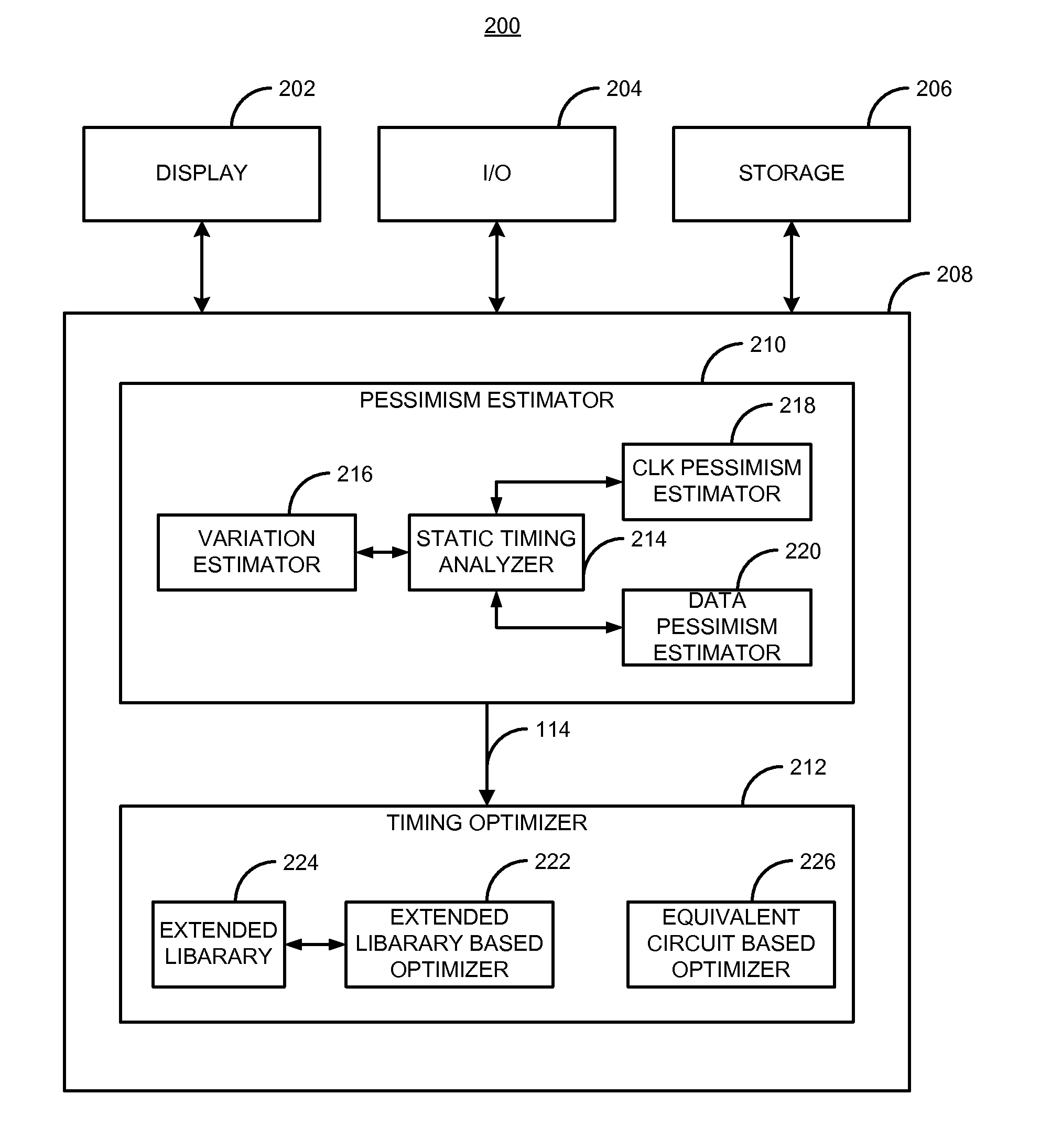
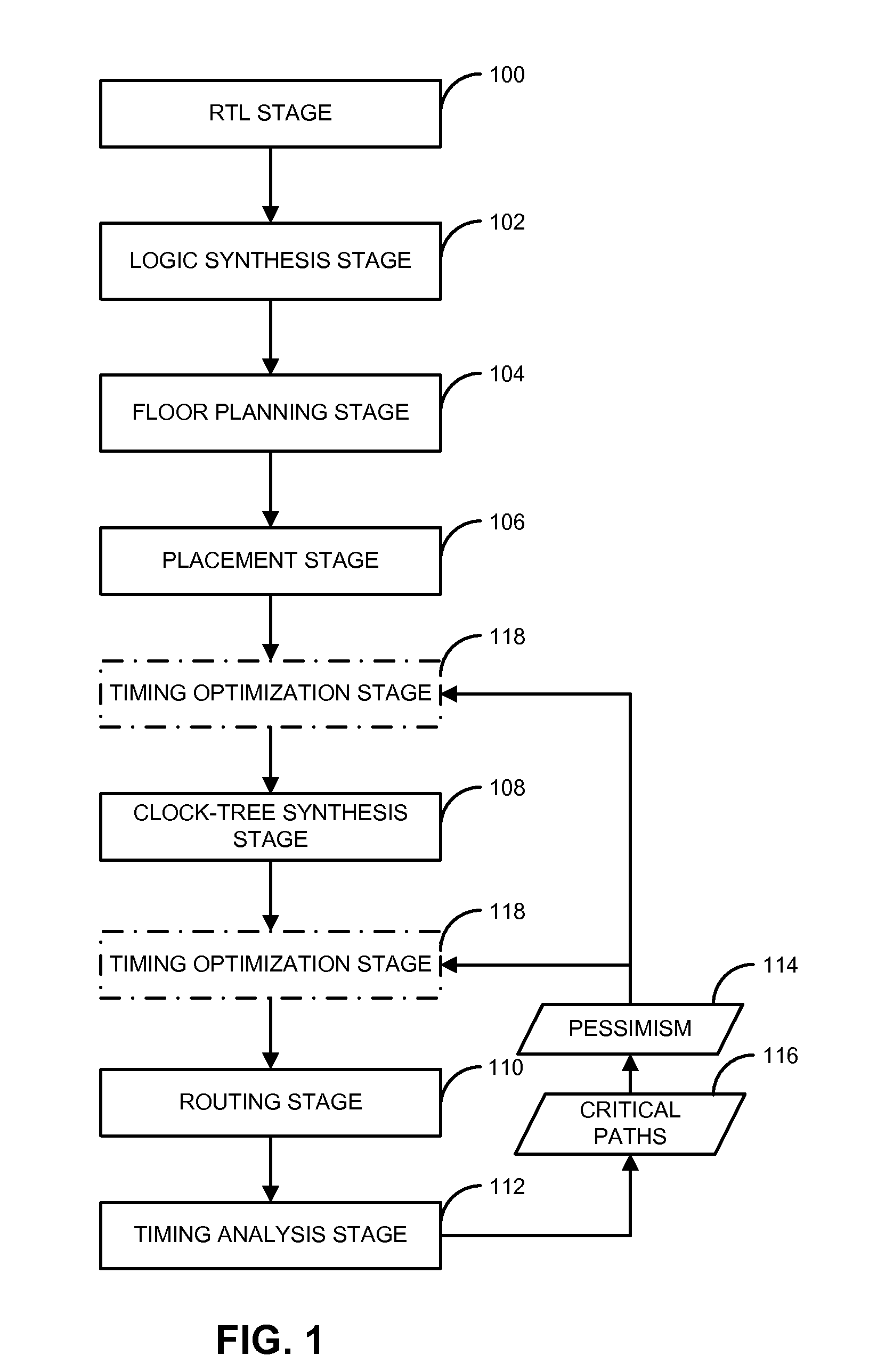
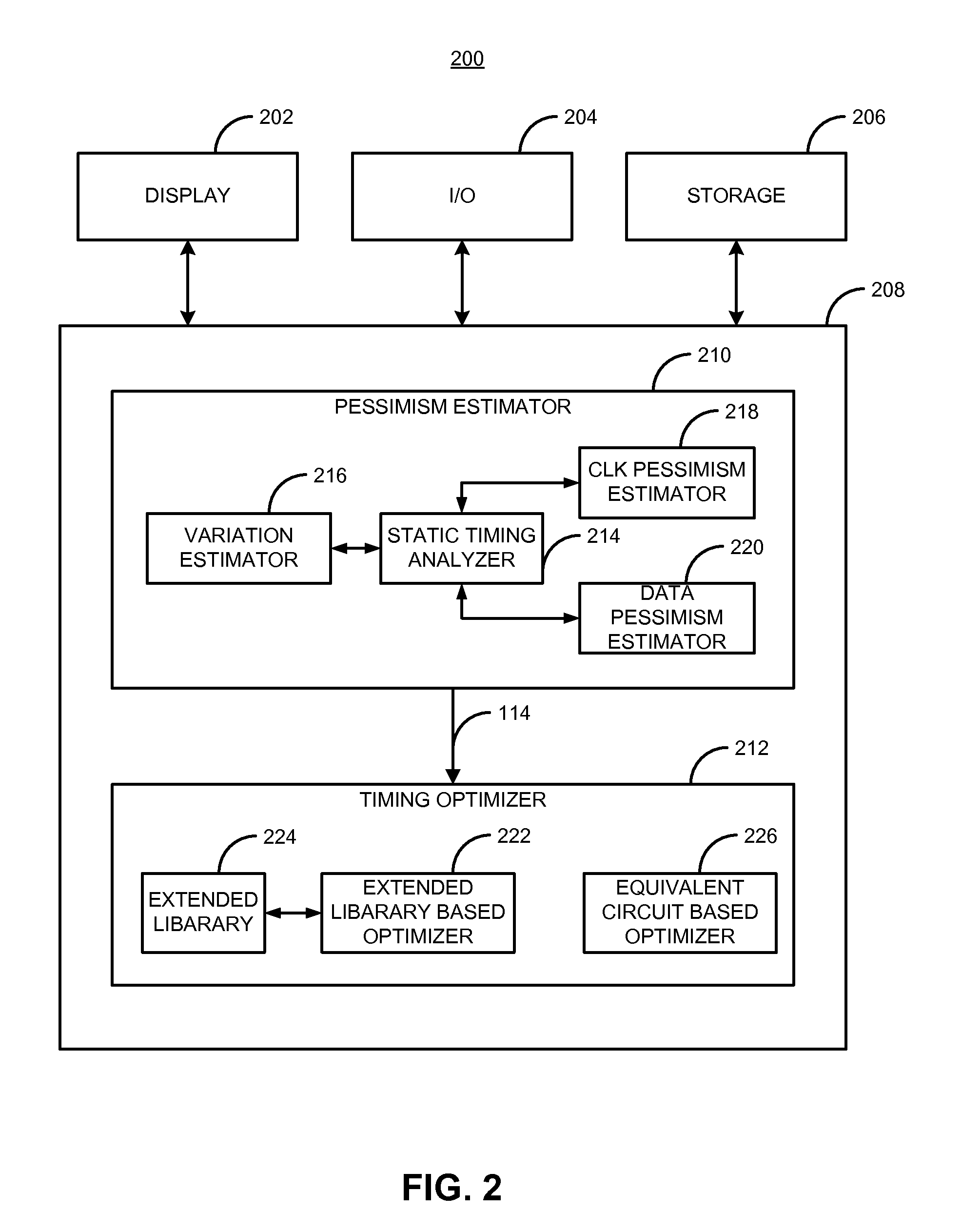
[0021]Briefly, in one example, a method and apparatus for designing an integrated circuit to operate at a desired clock frequency range reduces process variation by estimating the value of removable pessimism from a static timing analysis. The pessimism includes, for example, at least one of the removable on-chip-variation (OCV) margin from clock paths, removable OCV margin from data paths, removable IR drop margin from clock paths, and removable interconnects margin. At the timing analysis stage of a design flow, the method and apparatus determines the value of pessimism in the timing critical paths based on timing correlation between adjacent timing critical paths. In response to the determination, the value of pessimism may be reduced in the static timing analysis of the adjacent timing critical paths to optimize the timing performance of the integrated circuit at its desired clock frequency range.

[0022]Among other advantages, for example, the method and apparatus provides the ab...


PUM


Abstract

A method and apparatus for designing an integrated circuit to operate at a desired clock frequency range reduces process variation by estimating the value of removable pessimism from a static timing analysis. The pessimism includes, for example, at least one of the removable on-chip-variation (OCV) margin from clock paths, removable OCV margin from data paths, removable IR drop margin from clock paths, and removable interconnects margin. At the timing analysis stage of a design flow, the method and apparatus determines the value of pessimism in the timing critical paths based on timing correlation between adjacent timing critical paths. In response to the determination, the value of pessimism may be reduced in the static timing analysis of the adjacent timing critical paths to optimize the timing performance of the integrated circuit at its desired clock frequency range.

Description

CROSS-REFERENCE TO RELATED APPLICATION[0001]The present patent application claims priority from and the benefit of Indian Patent Application No. 1314 / DEL / 2011, filed May 5, 2011, and entitled METHOD AND APPARATUS FOR DESIGNING AN INTEGRATED CIRCUIT, which is hereby incorporated herein by reference.BACKGROUND OF THE DISCLOSURE[0002]The disclosure relates generally to a method and apparatus for designing an integrated circuit, and more particularly, to a method and apparatus for designing an integrated circuit to operate at a desired clock frequency range.[0003]Timing analysis and optimization is a design process by which an integrated circuit design is characterized and modified to meet its timing requirement in order to assure the fabricated integrated circuit will operate at the desired clock frequency range. However, the scaling down of fabrication process technologies has increased the process variation that impacts the frequency performance of integrated circuits by reducing the...

Claims


Application Information

Patent Timeline
Patent Type & Authority Applications(United States)
IPC IPC(8): G06F17/50
CPCG06F2217/62G06F17/5031G06F30/3312G06F30/396G06F30/3315
Inventor IYER, ARUNSHARIFF, YOUSUFF MOHAMMED
Owner ADVANCED MICRO DEVICES INC
Why Eureka
Try Eureka