System and method for analyzing power distribution using static timing analysis

a technology of static timing analysis and power distribution, applied in the direction of cad circuit design, program control, instruments, etc., can solve the problems of insufficient supply voltage, inoperable circuit, slow and, perhaps, inoperable circuit, etc., and achieve the effect of reducing the size of the chip and avoiding the problem of wiring congestion

Inactive Publication Date: 2004-12-14
MARVELL ASIA PTE LTD
View PDF5 Cites 26 Cited by
  • Summary
  • Abstract
  • Description
  • Claims
  • Application Information

AI Technical Summary

Benefits of technology

With its unique and novel features and designs, the inventive system and method provide fast and effective means for accurately analyzing the power distribution on an integrated circuit. The inventive system and method quickly and accurately predicts the current waveforms while not over-predicting them by so much that the product is grossly over-designed.

Problems solved by technology

Of course, insufficient supply voltage would make the circuit slow and, perhaps, inoperable.
Designers, on the other hand, must be careful not to overdesign the power distribution to each circuit because this would result in unnecessary chip size and wiring congestion.
This causes a problem, however, because, as the device threshold voltage (Vt) and power grid supply voltages (Vdd) are reduced, the ratios of noise voltages to Vt and Vdd increase because the noise levels do not scale down at the same rate as Vt and Vdd.
However, high current levels create local and often sizable resistive voltage drops in the power supply wiring.
In addition, increasing signal current levels and / or duty cycles further exacerbates the noise problems experienced in smaller chips and may also prevent the full Vdd supply voltage from being available to power some of the circuits on the chip.
However, this typically results in lower performance and / or increased power consumption, chip area and chip cost.
In addition, because noise sensitivity problems are often not realized until very late in the circuit design process and sometimes not until after the chips is actually fabricated, this method typically requires subsequent re-modeling / simulation and / or redesign activity which can be expensive and time consuming.
However, power distribution on a chip depends upon when and / or whether the various circuits on the chip will switch, which designers typically have no way of knowing with certainty.
Although this "worst case scenario" makes power distribution analysis relatively easy, it is not very accurate because many portions of the integrated circuit do not switch at the same time.
Therefore, the results would overstate voltage drops causing the chip to be over-designed.
However, numerous patterns are required here which makes analysis costly.
In addition, in spite of the numerous patterns, it remains likely that the maximum pattern (i.e., the pattern resulting in the maximum current for the circuit) will not be identified.
Furthermore, there inevitably will be patterns which were not conceived or impossible to generate that will cause more switching activity than modeled.
Therefore, this analysis commonly results in long analysis or design times and missed design errors.

Method used


Image

  • System and method for analyzing power distribution using static timing analysis
  • System and method for analyzing power distribution using static timing analysis
  • System and method for analyzing power distribution using static timing analysis

Examples


Embodiment Construction

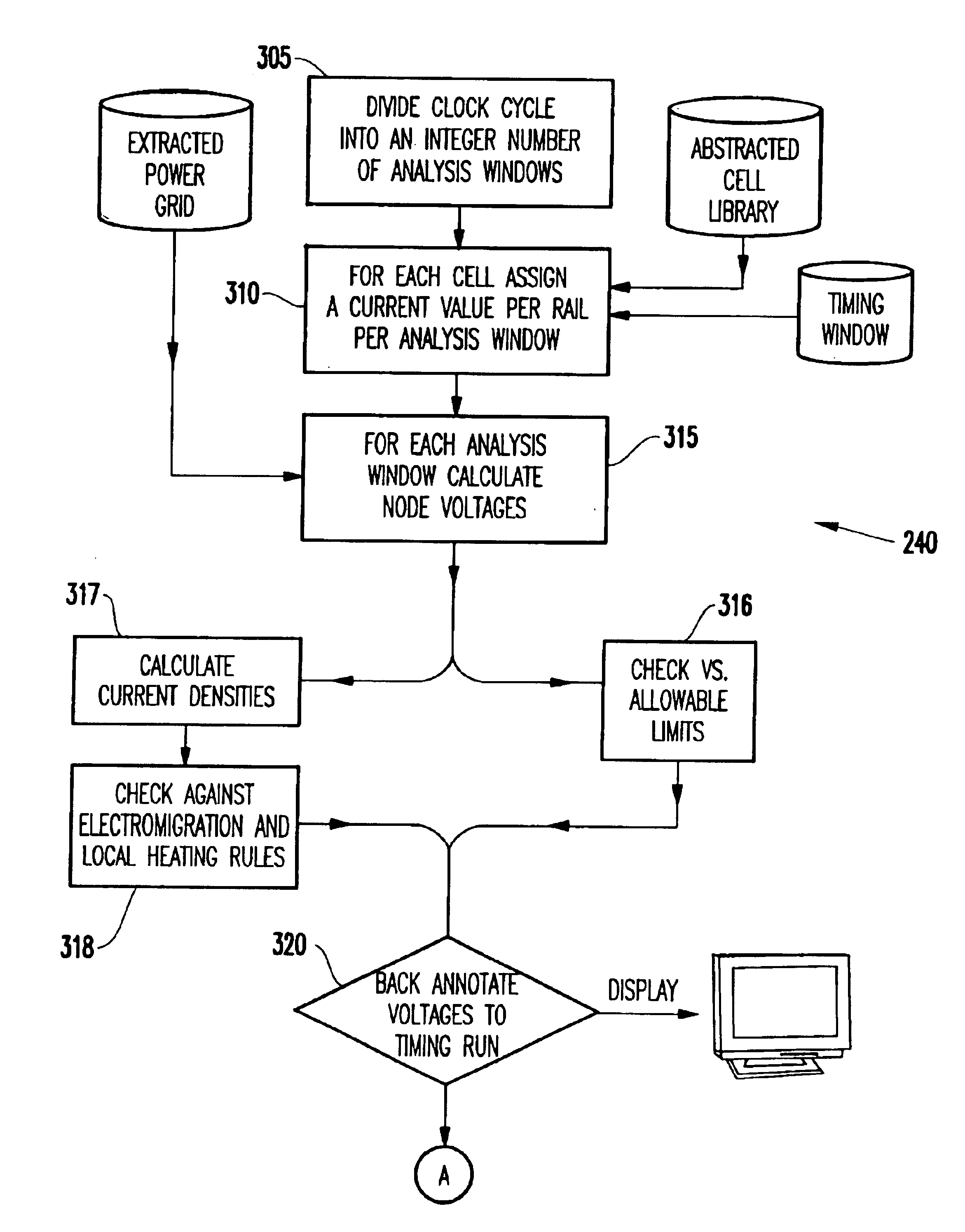
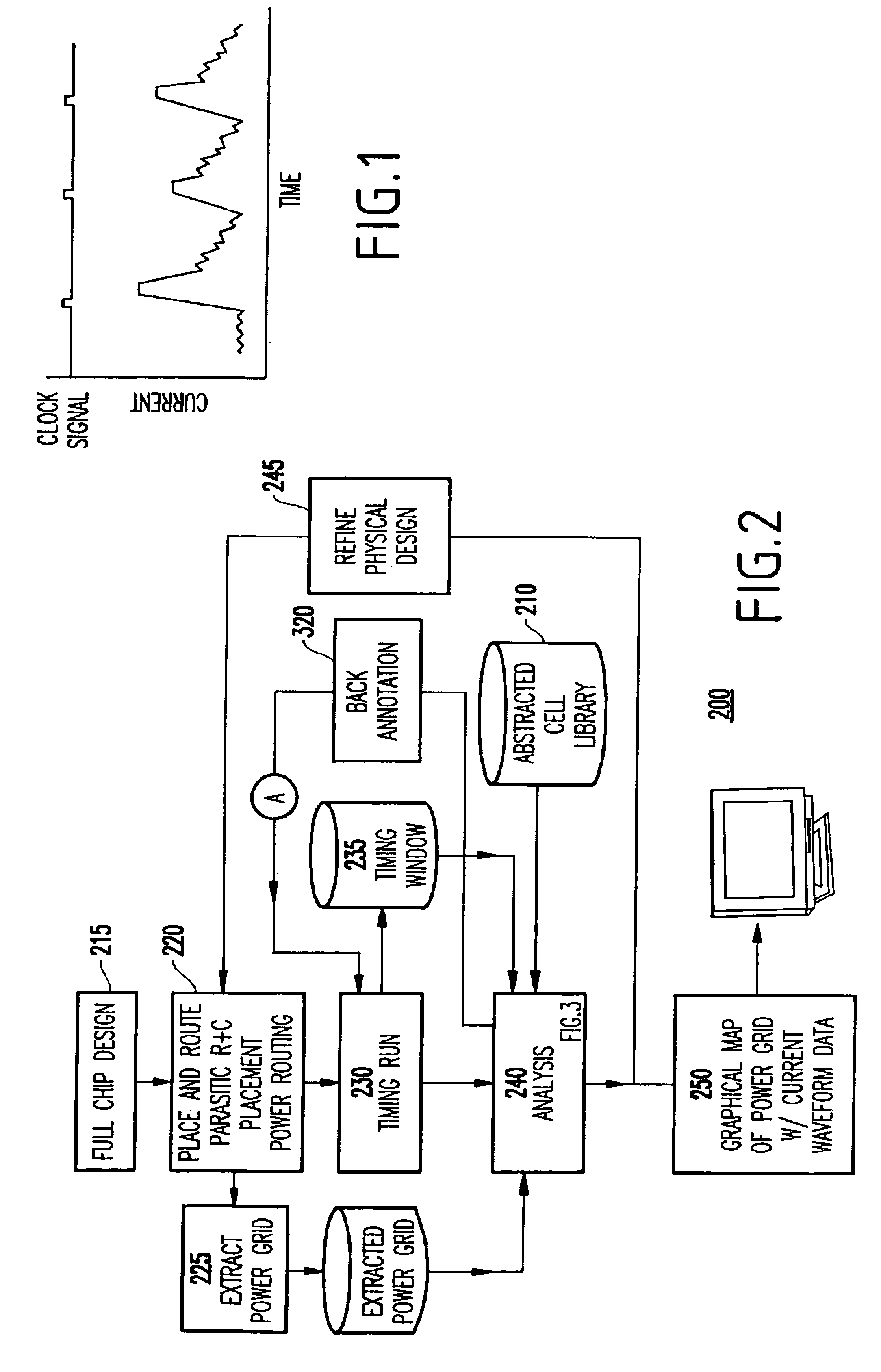
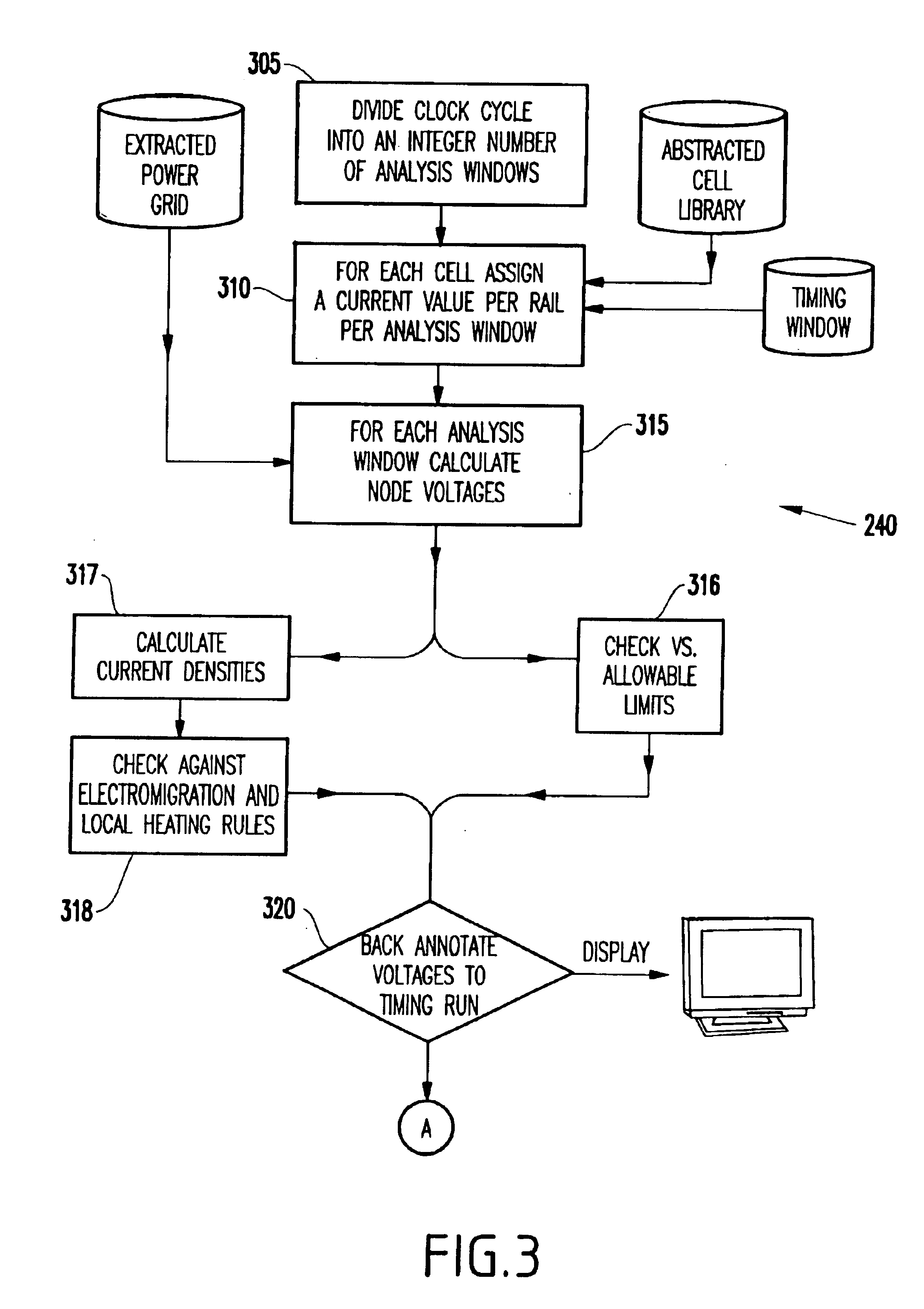
Referring now to the drawings, FIG. 2 is a flow diagram illustrating a method 200 of analyzing power distribution according to the present invention.

As noted above, to perform power distribution analysis, a designer must know when and / or whether the various circuits on the chip will switch, which designers typically have no way of knowing with certainty. However, the inventors have discovered that the following assumptions can be made with respect to when and / or whether a given circuit on the chip will switch to provide a simple yet effective power distribution analysis:

1. All circuits are switching in the same direction at the same time. This may be refined to exclude circuits that cannot possibly switch within a given interval. No attempt is made to determine which direction a circuit is switching as this would require information about "patterns" which is often not available to the designer or the customer.

2. All circuits are switching in the same direction. First, it is assumed ...


PUM


Abstract

A method and system for analyzing power distribution in an integrated circuit chip includes dividing a clock cycle of the integrated circuit chip into a plurality of time periods, dividing the integrated circuit chip into a plurality of cells, performing a static timing analysis for the plurality of cells to obtain current waveform data for each cell and each time period, and performing a power distribution analysis using the current waveform data.

Description

1. Field of the InventionThe present invention relates generally to a system and method for analyzing power distribution in an integrated circuit and more particularly, to a system and method for analyzing power distribution by using static timing analysis to calculate current waveforms.2. Description of the Related ArtFIG. 1 provides a graphical representation of current in a typical integrated circuit chip over time. As indicated in FIG. 1, the current in the circuit rises to a peak sometime after the clock edge, and then gradually tapers off to near zero until the next clock edge occurs (assuming complementary metal oxide semiconductor (CMOS) logic). The height of each peak is a function of the number, location, and type of circuits switching. These parameters are controlled by the logical function of the chip and the data being supplied to the chip and can change on each subsequent clock cycle.One goal of chip design is to optimize the power distribution on the chip so that each...

Claims


Application Information

Patent Timeline
Patent Type & Authority Patents(United States)
IPC IPC(8): G06F17/50H01L21/82
CPCG06F17/5022G06F30/33
Inventor COHN, JOHN MAXWELLGOULD, SCOTT WHITNEYROSE, RONALD DENNISWEMPLE, IVANZUCHOWSKI, PAUL STEVEN
Owner MARVELL ASIA PTE LTD
Why Eureka
Try Eureka