Vertical cavity surface emitting laser diode having a high reflective distributed Bragg reflector

a laser diode and vertical cavity technology, applied in semiconductor lasers, optical resonator shape and construction, laser details, etc., can solve the problems of increasing the size of the vcsel, reducing the reflectivity of the latter method, and limiting the application of materials

Active Publication Date: 2008-02-12
SUMITOMO ELECTRIC IND LTD
View PDF12 Cites 3 Cited by
  • Summary
  • Abstract
  • Description
  • Claims
  • Application Information

AI Technical Summary

Benefits of technology

[0009]The first semiconductor layer may be a GaAs layer, and the aluminum oxide layer may be formed by the oxidization of at least one of AlAs layer and AlGaAs layer. These aluminum containing semiconductor materials have lattice constants substantially matching to that of GaAs, and a difference in the refractive index of the oxide form, i.e., the aluminum oxide, with that of GaAs becomes far greater than those of not oxidized form. Therefore, when such aluminum oxide layer converted from the semiconductor material is used in the DBR, the number of pairs of the first semiconductor layer and the aluminum oxide layer can be reduced. In the present invention, the number of pairs may be reduced at least five (5).
[0010]The DBR of the present invention may further include a plurality of second semiconductor layers in a peripheral region of the aluminum oxide layer. The first semiconductor layer may be divided into the center region and the peripheral region. The aluminum oxide layer may be provided on the center region, while the second semiconductor layer may be provided on the peripheral region. Since the adhesion between semiconductor materials is stronger than that between the semiconductor material and the aluminum oxide material, this configuration effectively prevent the aluminum oxide layer from peeling off the first semiconductor layer.
[0011]The present VCSEL may further include a third DBR between the second DBR and the active layer. This third DBR comprises a plurality of pairs comprises of a third and a fourth semiconductor layer, both of which may be substantially lattice matched to said substrate and also lattice miss-matched to said first semiconductor layer. The second DBR may mechanically attached to the third DBR. Accordingly, even the semiconductor material constituting the second DBR has lattice constant mismatched to the semiconductor substrate, the DBR with enough reflectivity may be obtained.

Problems solved by technology

However, when semiconductor materials are used to form these two layers in the DBR, taking the lattice constant of two layers adjacent to each other into account, applicable materials are quite restricted.
Therefore, it is considerably hard to take the latter method to increase the reflectivity.
Accordingly, the former method, namely to increase the number of layers, has been an available solution, which increases the size of the VCSEL and complicates the process thereof.

Method used


Image

  • Vertical cavity surface emitting laser diode having a high reflective distributed Bragg reflector
  • Vertical cavity surface emitting laser diode having a high reflective distributed Bragg reflector
  • Vertical cavity surface emitting laser diode having a high reflective distributed Bragg reflector

Examples


first embodiment

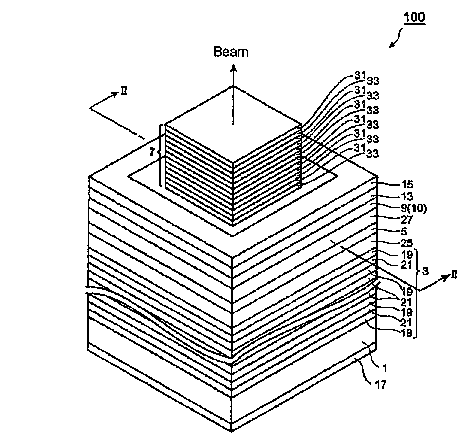
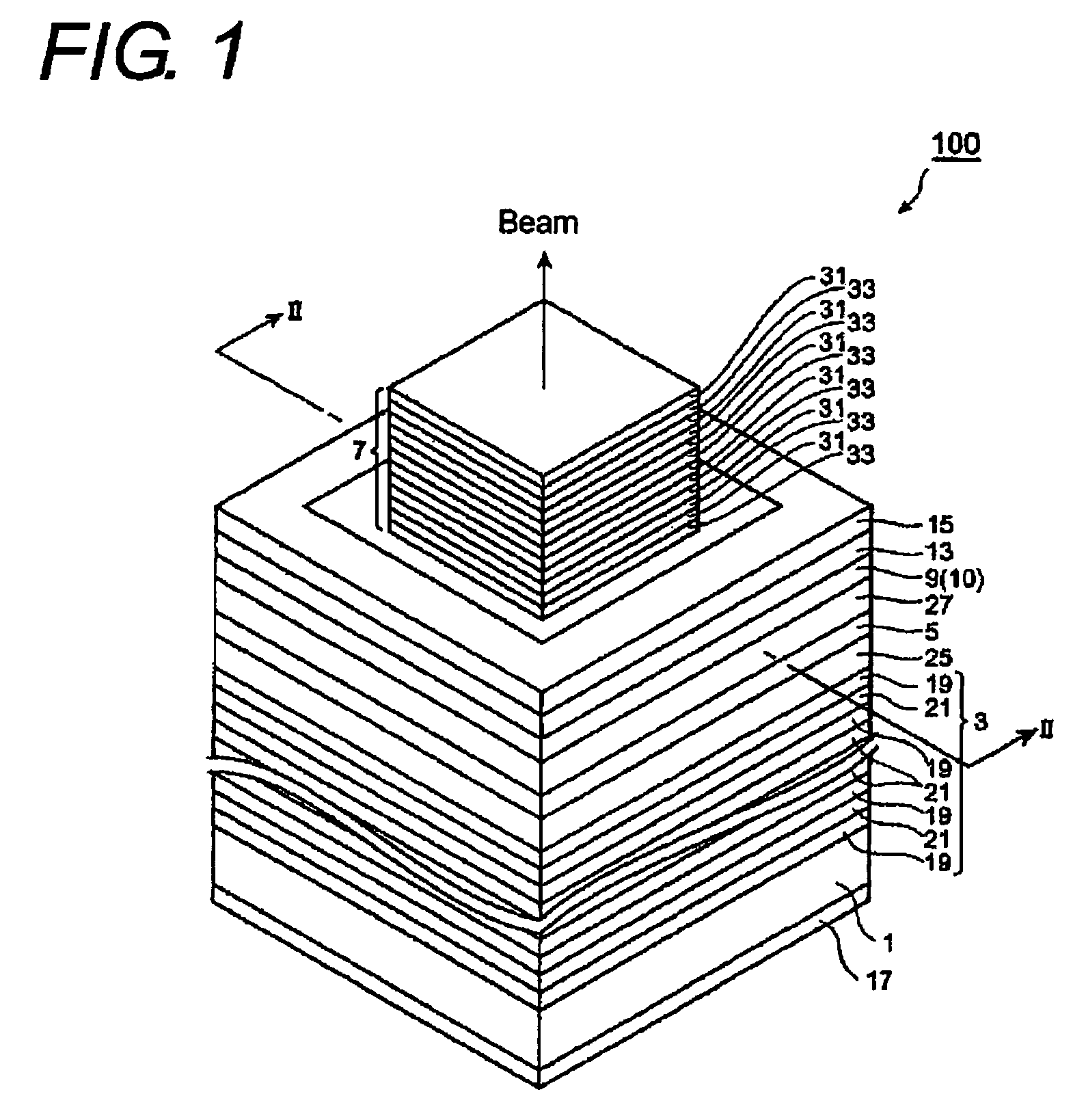
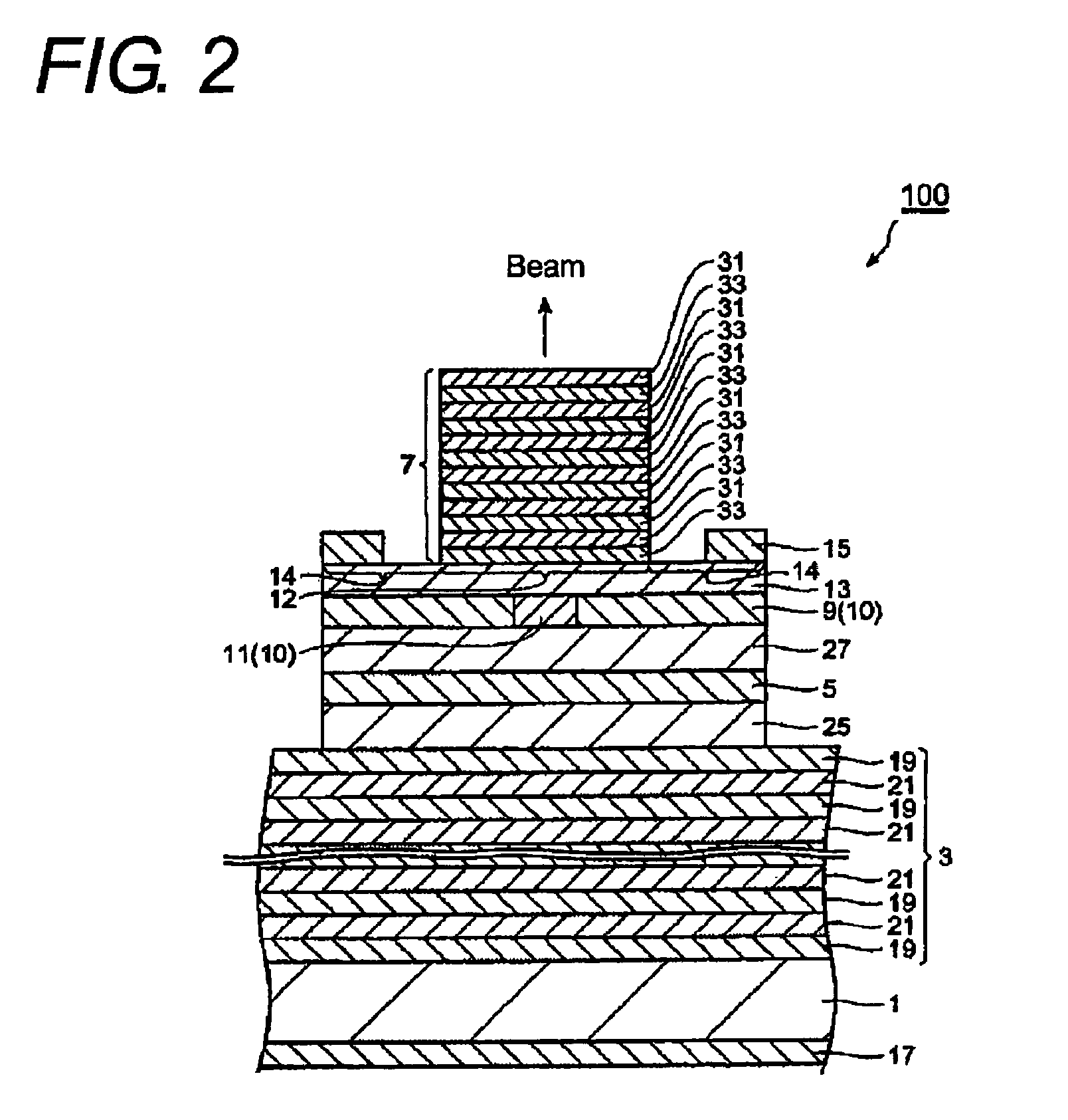
[0034]FIG. 1 is a perspective view schematically showing a vertical cavity surface emitting laser diode (VCSEL) 100 according to the first embodiment of the present invention, and FIG. 2 is a cross section of this VCSEL taken along the line II-II in FIG. 1.

[0035]The VCSEL 100 provides a lower distributed Bragg reflector (DBR) 3, an upper DBR 7 and an active layer 5 between the lower and upper DBRs. Between the active layer 5 and the lower DBR 3 is provided with a first AlGaAs layer 25, while between the active layer 7 and the upper DBR 7 is provides with a second AlGaAs layer 27. The first and second AlGaAs layers, accompanied with the active layer 5, form an optical cavity with a thickness of one wavelength λ.

[0036]Between the second AlGaAs layer and the upper DBR 7 is preferably provided with a current confinement layer 10. This current confinement layer 10 has a center portion 11 for passing the current and a peripheral portion 9 surrounding the center portion 11. The center port...

second embodiment

[0063]FIG. 8 is a cross section showing another VCSEL 200 according to the second embodiment of the invention. The VCSEL 200 of the second embodiment has an n-type InP substrate 201, a lower DBR 203, an upper DBR 7, and an active layer 205 between the lower and upper DBRs, 203 and 7, respectively.

[0064]The lower DBR 203 comprises n-type InGaAsP layers 219 doped with Si and n-type InP layers 221 doped with Si alternately stacked to each other. In this embodiment, twenty six (26) n-type InGaAsP layers 219 and twenty five (25) n-type InP layers 221 are stacked. Therefore, the uppermost and lowermost layers of the lower DBR 203 are the n-type InGaAsP layer 219.

[0065]The thickness of the n-type InGaAsP layer 219 is preferably λ / 4 / nr10, while that of the n-type InP layer 211 is preferably λ / 4 / nr11, where λ, nr10, and nr11 are the emitting wavelength of this VCSEL 200, the effective refractive index of the n-type InGaAsP and the n-type InP, respectively.

[0066]The upper DBR 7 has the simila...

third embodiment

[0077]Next, another VCSEL 300 according to the third embodiment of the invention will be described. FIG. 9 is a schematic cross section showing the third VCSEL 300 of the invention. The VCSEL 300 includes the lower DBR 3 and the upper DBR 7, both provided on the n-type GaAs substrate. Between the lower and upper DBRs is provided with the active layer 5.

[0078]The VCSEL 300 provides an upper DBR 307 whose structure is different to that of the upper DBR 7 of the first embodiment shown in FIG. 2. That is, the upper DBR 307 of this embodiment provides a plurality of GaAs layers 31, each GaAs layer 31 including a center region 37 and a peripheral region 35 surrounding the center region 37. On the center region 37 of respective GaAs layers 31 is provided with the aluminum oxide layer 33, while another semiconductor layer 32 is provided on the peripheral region 35. The another semiconductor layer 32 includes at least one of AlGaAs or AlAs. Adhesion between the GaAs layer 31 and the semicond...


PUM


Abstract

The present invention is to provide a vertical cavity surface emitting laser diode (VCSEL) that has a functional distributed Bragg reflector (DBR) comprised of less number of pairs of reflective layers. The VCSEL of the invention include a lower DBR, an upper DBR and an active layer arranged between the upper and lower DBRs. The upper DBR is comprised of a plurality of pairs including GaAs layers and aluminum oxide layers, thus the GaAs layers and the aluminum oxide layers are alternately stacked to each other. Since the refractive index of the aluminum oxide (Al2O3) is 1.67 at 1.3 μm and that of the GaAs is 3.51, the difference of these refractive index becomes 1.85, which is far greater than the combination of the AlAs and the GaAs, thereby decreasing the number of pairs for the DBR.

Description

BACKGROUND OF THE INVENTION[0001]1. Field of the Invention[0002]The present invention relates to a vertical cavity surface emitting laser diode (hereinafter denoted as VCSEL), in particular, relates to a structure of a mirror defining a cavity of the VCSEL.[0003]2. Related Prior Art[0004]The VCSEL enables to emit light with nearly circular field pattern because the VCSEL emits light from the primary surface of the semiconductor layer, not from an end surface thereof. Moreover, the VCSEL in particular the active portion thereof, may be integrated on single substrate with high density.[0005]The VCSEL provides a lower mirror and an upper mirror on a GaAs substrate, between which an active layer is sandwiched. In one of prior VCSELs, these lower and upper mirrors have a structure of alternately stacked AlAs layer and GaAs layer. These mirrors operate and are called as a distributed Bragg reflector (DBR).[0006]These upper and lower DBRs should have relatively high reflectivity to emit co...

Claims


Application Information

Patent Timeline
Patent Type & Authority Patents(United States)
IPC IPC(8): H01S3/08H01S5/00H01S5/183H01S5/187
CPCH01S5/187H01S5/18308H01S5/18341H01S5/18361H01S5/18372H01S5/1835
Inventor TAKAHASHI, MITSUO
Owner SUMITOMO ELECTRIC IND LTD
Why Eureka
Try Eureka