Semiconductor device and testing method for same

a technology of semiconductors and devices, applied in the field of semiconductor devices, can solve problems such as the increase of dram products after shipment, and achieve the effect of reducing the number of errors of dram products

Inactive Publication Date: 2008-03-18
PS4 LUXCO SARL
View PDF13 Cites 26 Cited by
  • Summary
  • Abstract
  • Description
  • Claims
  • Application Information

AI Technical Summary

Benefits of technology

[0026]It is therefore an object of the present invention to provide a semiconductor device that allows error correction of a pattern of bits that are already uncorrectable and that are the objects of remedy by redundancy, and a pattern of bits that are uncorrectable due to the addition of single-bit fail bits.
[0027]It is another object of the present invention to offer a semiconductor device testing method that allows the error correction of a pattern that is already uncorrectable and that is the object of remedy by redundancy and a pattern that is uncorrectable due to the addition of one-bit fail bits.
[0047]The present invention therefore enables the determination of a pattern that is already uncorrectable, and, a pattern that becomes uncorrectable due to, for example, the addition of single-bit fail bits, and consequently, enables the remedying of potential defective cells in an examination process such as a wafer inspection.

Problems solved by technology

The additional errors of DRAM products following shipment increase due to the addition of single-bit fail bits, and this problem calls for an effective countermeasure.

Method used


Image

  • Semiconductor device and testing method for same
  • Semiconductor device and testing method for same
  • Semiconductor device and testing method for same

Examples


Embodiment Construction

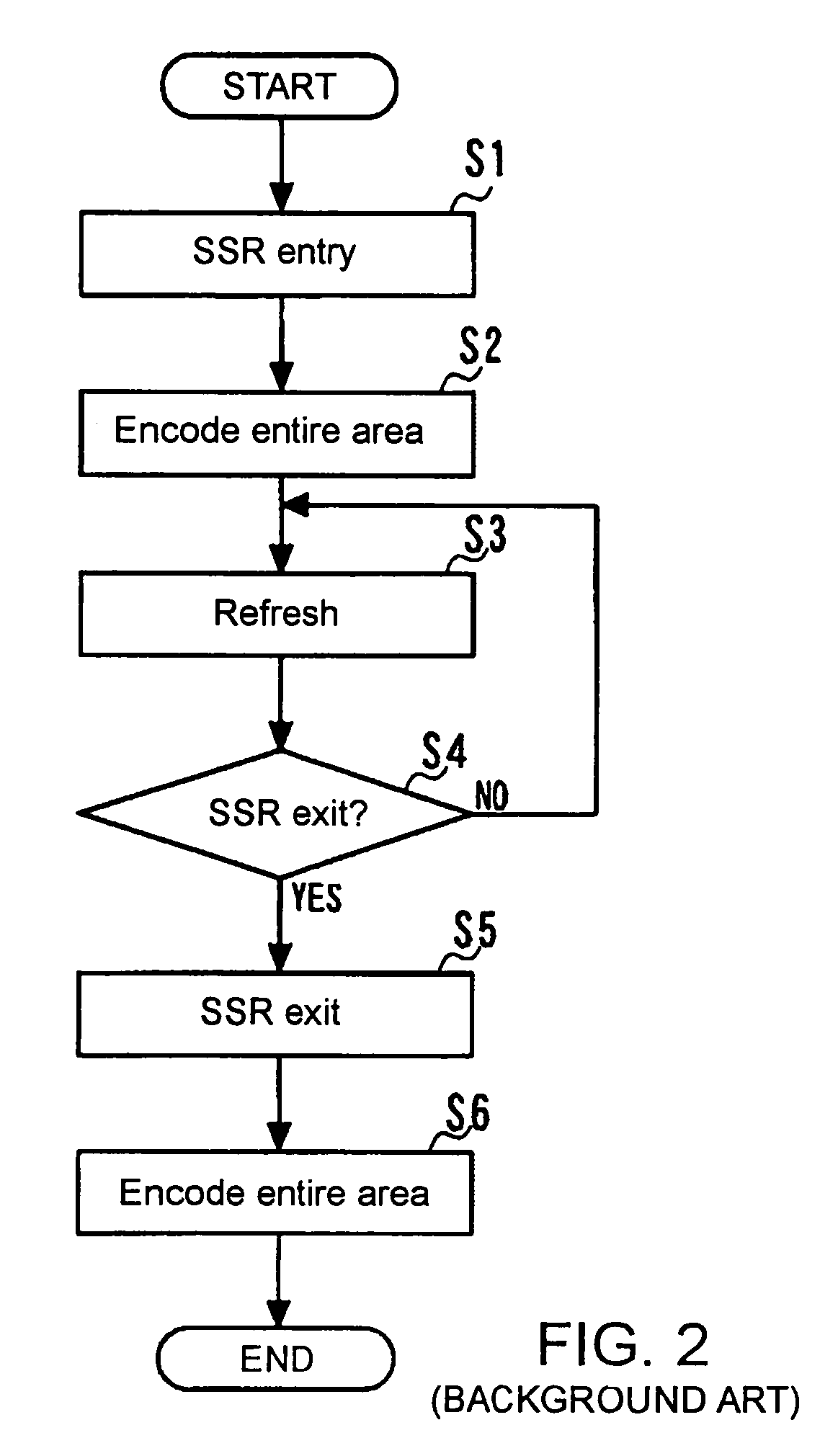
[0075]FIG. 9 shows the procedures for remedying defective cells according to an embodiment of the present invention in comparison with the procedure of the prior art. In FIG. 9, flow 309A shows the procedure of the prior art that is shown in FIG. 5 Without alteration, flow 309B shows the first procedure based on the present invention, and flow 309C shows the second procedure based on the present invention.

[0076]In the first procedure, as shown in flow 309B, all bits are first written at a prescribed value (ALL 1) in Step S21; and then encoded by means of only code #1 in Step S22. A refresh operation is then carried out at a refresh cycle of tREF=1 second in Step S23.

[0077]Next, in Step S24, all bits are read from the memory cell array and decoded by code #1, and pass / fail of the data is determined in Step S25. The addresses of fail bits that are obtained from the results are recorded in the first fail memory (Fail Memory #1) that is installed in memory tester (not shown).

[0078]Next,...


PUM


Abstract

A test method for a semiconductor device that is provided with an ECC circuit that uses product code that is composed of a first code and a second code for implementing error correction of a memory, the test method includes steps of: obtaining first pass / fail determination results and second pass / fail determination results that are realized by independent correction operations based on the first code and the second code, respectively; recording the results in a first fail memory and a second fail memory, respectively; executing a prescribed logical operation such as an AND operation relating to the contents of the first fail memory and the contents of the second fail memory; and based on the results of the logical operation, remedying both fail bits and potential fail bits.

Description

BACKGROUND OF THE INVENTION[0001]1. Field of the Invention[0002]The present invention relates to a semiconductor device that is provided with memory, and more particularly to a semiconductor device that is provided with a product code ECC (Error Checking and Correcting) circuit for correcting errors in memory, and to a method of testing such a device.[0003]2. Description of the Related Art[0004]Of the various methods that are used in a dynamic semiconductor memory device that requires a refresh operation to hold data, the Super Self Refresh (SSR) technology can extend the refresh cycle to as much as approximately one second when the ambient temperature Ta is 85° C., by both arranging an ECC circuit on a semiconductor memory device and then encoding the entire chip area at the time of entry to a low-consumption power mode and implementing a correction operation of the entire chip area at the time of exit from the low-consumption power mode. The SSR technology is disclosed in, for exa...

Claims


Application Information

Patent Timeline
Patent Type & Authority Patents(United States)
IPC IPC(8): H03M13/00H03M13/01G06F11/00G06F11/10G11C11/401G11C11/406G11C11/4078G11C29/00G11C29/42H03M13/29
CPCG06F11/1012G06F11/1076G11C11/406G11C29/42G11C2211/4062
Inventor RIHO, YOSHIROITO, YUTAKA
Owner PS4 LUXCO SARL
Why Eureka
Try Eureka